| John Broskie's Guide to Tube Circuit Analysis & Design |
12 August 2006
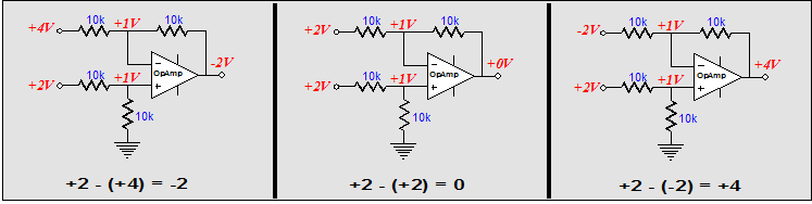
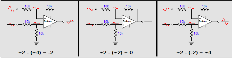
Balanced-Ouput DACs and Tubes Back to DACs. Last time we looked at this topic, we saw tube circuits picking up their input signal from DACs with a single output, which was either a voltage or a current output. So far, everything has been fairly straightforward; however, when we come to DACs with balanced outputs, we face a few twists. For example, most CD players and stand-alone DAC units that sport balanced-output DACs are not balanced themselves at their outputs, with a single RCA jack per channel as an output. Here is another oddity: the output of a non-balanced DAC is usually referenced to ground, with an output that expects to see 0V. On the other hand, balanced outputs are usually referenced to some positive voltage, say 2.5V. So, the first question is: Why use balanced-output DACs when the final output is unbalanced? The answer is that we can get better performance at less cost. When the DAC's two phases of output signal are summed together, the summing circuit’s intrinsic common-mode rejection ration (CMRR) will ignore the noise that is common to each balance output, amplifying only what is not common in its single-ended output, which affords an improved signal-to-noise ratio. In other words, the power-supply noise falls out of the mix, so a simpler and cheaper DAC power supply is allowable. CMRR and differential amplifiers are seldom mentioned in tube circles. The following illustrations expose a differential amplifier’s functioning.
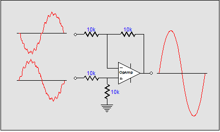
Now, we can see how the differential amplifier, by ignoring what is common and amplifying what is different between balanced inputs, can produce a clean output waveform from two dirty signals. (Note that when both inputs see the same voltage, the output falls to zero.)
The next question is: Why do so many new DACs have outputs that are not at the ground potential? Historically, the trajectory that DACs have been on started with many pins and many support devices and many supply voltages to the desired end of only a few pins and only one power supply voltage. The reasoning is easy to decipher—it’s both easier and cheaper that way. The makers of digital-audio gear complained of the cost of all the required prop-up components, such as decoupling capacitors and trimming potentiometers, and excessive complexity (they had been spoiled by OpAmps, which are cheap and easy to use); and the makers of DACs wearied of the many user-support headaches, as their DACs failed to deliver the advertised performance due to their customers' lack of understanding and sloppy construction practices. In other words, no one was happy. Thus, we are getting DACs that are simpler, cheaper, and easier to implement.
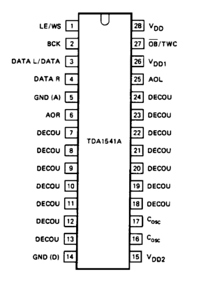
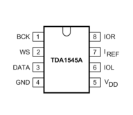
In the above DAC footprints, we can see the move to smaller and simpler. (Each of the pins labeled "DECOU" and pins 16 and 17 require shunting capacitors; and the DAC requires three power supply voltages, +5V, -5V, and +15V.) However, a single power supply voltage of 5V cannot accommodate a ground-voltage-referenced output, as there is no negative-power-supply voltage to support a current source to pull the output down to ground level. (If the output were inductively loaded, however, such a DAC would become possible; but who— other than an audiophile —wants an expensive, heavy, hum-attracting choke in his or her iPod or portable CD player?) Thus, many of the new, streamlined DACs have an output referenced, not to ground, but instead at B+ voltage divided by two (or some value close to two). For example, if the DAC’s power supply voltage is 5V, then its signal outputs will be at +2.5V. So is a coupling capacitor needed to block this large DC offset? No, because the balance-to-unbalanced circuit will drop out the 2.5V DC offset along with the noise, as the shared DC offset voltage is effectively a common mode signal. So where the old DACs were complex, requiring many clean power-supply voltages and many bypassing capacitors, the new breed of easy-to-use DACs requires only one power supply voltage, and it need not be perfectly clean for a fairly decent PSRR.
Tubes to the rescue 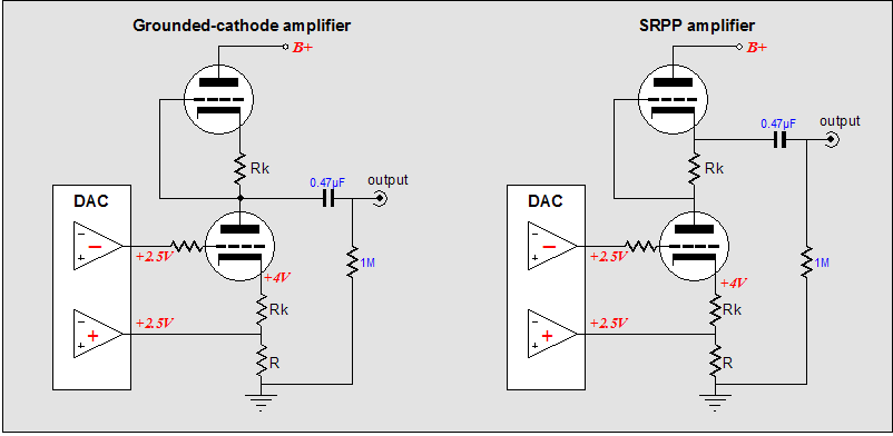 In both circuits, the addition of resistor R in the cathode circuit, allows the tube circuit to have its effective reference voltage upped to 2.5V. 
In other words, without the DAC, the tube circuit would bias up to where the connection between RK and R would naturally sit at 2.5V at idle. Of course, we are not limited to the two above tube circuits. For example, the Aikido amplifier can be used just as easily: 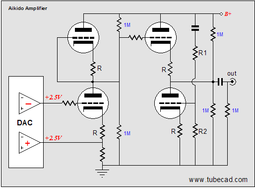 The input stage of the Aikido is effectively lifted 2.5V off ground by the addition of the extra resistor. By switching to the Aikido we gain all the benefits that the Aikido offers, such as low output impedance, low distortion, and a great PSRR. The only obvious problem is that of too much gain (the previous two circuits also suffer from this), as the balanced signal from the DAC will result in twice the gain we would have gotten from a comparable unbalanced signal source. In the case of the Aikido, the calculation is an easy one: gain roughly equals amplification factor of the input tube, for example, 20 for the 6SN7 and 33 for the 6922. Another less obvious problem that we might encounter with all these circuits is that the wimpy internal OpAmps in the DAC might not be able to drive such a low-impedance load. Which low-impedance load? The non-inverting outputs (in these schematics at least) have the low-valued resistor that bridges the cathode resistor to ground. This resistor is also in parallel with the low output impedance presented by the bottom triode's cathode in series with the cathode resistor. What can be done? The following circuit unloads the internal OpAmps by the current gain of the transistors used (typically, well over 100). 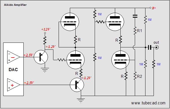
Oh my, how amazingly creepy: two transistors! Try as I may, I keep forgetting that if a nervous audiophile cannot see a transistor, such as the several hundred in the DAC, the transistors do not exist. Okay now, is there a circuit that isn't so creepy and doesn't have excessive voltage gain and doesn't burden the internal OpAmps within the DACs? (This would be much more dramatic with a beautiful, scantly-clad, showgirl assistance and a shower of sparks...) 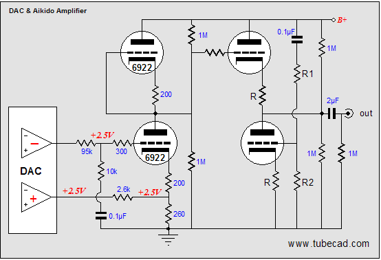
What we are doing here is throwing away much of the DAC's output signal, while providing a higher-impedance load to the DAC, and while retaining the high CMRR. Extra touches can take the form of high-frequency-shunting capacitors added to filter away some of the high-frequency noise from the DAC. 
(The same buffer/attenuator circuit can be used with the first two circuits shown, the grounded-cathode and SRPP amplifiers.) On the other hand, if no gain is required, then a much simpler circuit can be used. (Remember, no gain, no pain.)
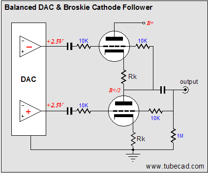
The Broskie cathode follower has been covered here before, so only a quick recap will be given. This circuit accepts a balanced input, which it converts to an unbalanced, single-ended output (the circuit itself is push-pull in functioning). It offers low distortion and low output impedance and, most importantly in this discussion, a good CMRR figure. 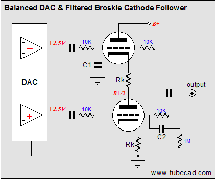
The Broskie CF can accommodate a low-pass filter by adding two capacitors, C1 and C2. These capacitors limit the high-frequency bandwidth, which will help filter away high-frequency DAC generated noise. (I would place the transition frequency at 30kHz with 500pF capacitors.)
Next time //JRB
|
|


| www.tubecad.com Copyright © 1999-2006 GlassWare All Rights Reserved |