| John Broskie's Guide to Tube Circuit Analysis & Design |
26 June 2016
Recap Time
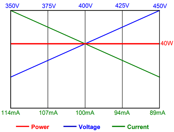
No doubt, more than a few readers find such an approach quaint, so analog, so old-fashioned in our digital age. Such a reader would find the alternative solution easy: use a small postage-stamp-sized CPU, such as the Arduino or BeagleBone or Raspberry Pi, and let it perform ADC transformations on the B+ voltage and idle current, so that the digital data can be processed by software and the corrected bias-voltage fed from a DAC internal to the CPU. Super simple, super cheap. Or at least so it is believed, as I am inclined to see such a project transform into something far more complicated and expensive than one first imagined. But if you fancy that you are up to it, please go for it. I would love to hear about your results. One other question that must also come to mind is, Just how constant is constant power? Ideally, the following RED graph plotline would result.
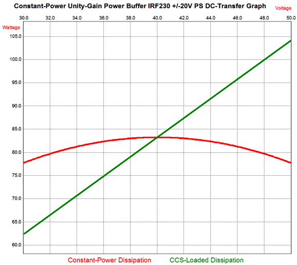
In spite of a 100V shift in B+ voltage, the plate dissipation remains fixed at 40W. In contrast, in my last post, I showed plotlines that looked like this:
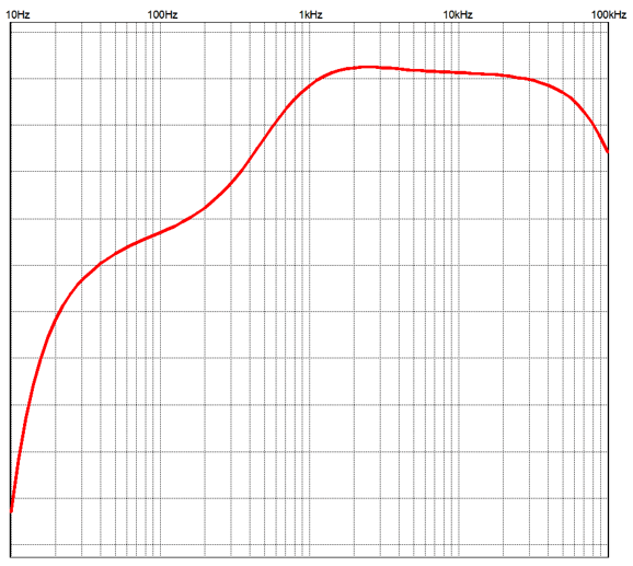
Not very flat. Or is it? Just like statistics, graphs can deceive. For example, would you buy a phono stage whose frequency response looked this lumpy?
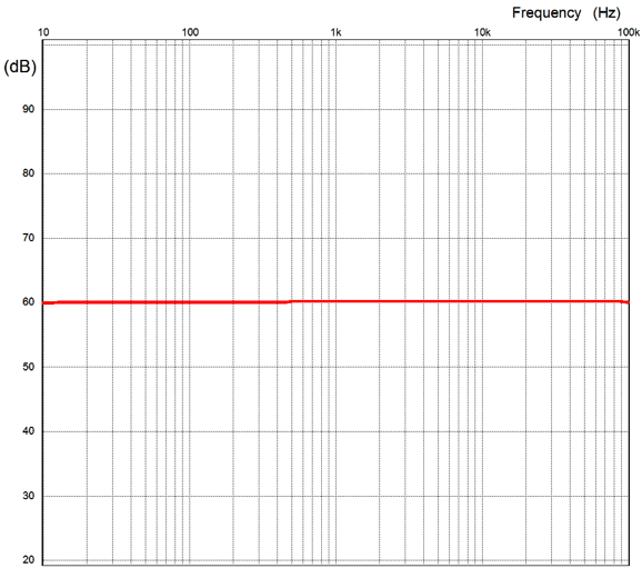
No bass, no slam. Probably not. On the other hand, the following phono-stage frequency response graph looks much more promising.
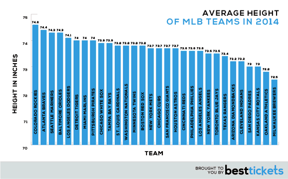
Of course, both graphs are of the exact same plot line, but with varying Y-axis increments. Both plotlines reveal a frequency response from 20hz to 20khz that deviates no more than 0.1dB. Do a quick search on Google and you will find many examples of deceptive graphs, such as those that exclude a portion of the data, which makes the difference between plotlines appear exaggerated, such as the following from besttickets.com.
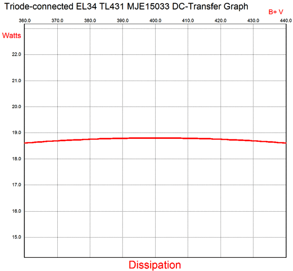
This graph shows the average height of major-league baseball players based on team. My gosh, those Milwaukee baseball players are mere stumps of men compared to those towering Denver giants, as the plotline for Milwaukee Brewers is about 60% as long as the plotline for the Denver Rockies. (My home team, by the way.) Or, maybe not. Note that that the graph starts at 5 foot 10 inches, which is already higher than the average American man (i.e. 69.7 inches, or 5 foot 9.7 inches) and that the height of the average Milwaukee player is 6 foot and half an inch. In addition, the difference in average heights between shortest and tallest teams is only 2.1 inches. Indeed, it is quite possible that most of the Milwaukee players are actually taller than most of the Denver players. How could that be possible? When dealing with averages, just about anything is possible. For example, the Denver team might hold a pair of twins from Holland who stand 6 foot 8 inches, whereas the Milwaukee team might hold a pair of twins from Japan who stand 5 foot 6 inches. The result of these four height-outlying men could substantially skew the average heights. In other words, we really need to see a scatter chart that would include the heights of all the players on each team. Okay, let’s reexamine at a previously shown constant-power graph, but with whole-watt Y-axis increments.
In other words, it’s more than flat enough, as the plate dissipation deviates by only 1% from its target value at both extremes.
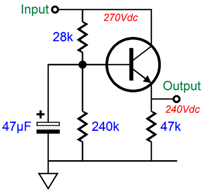
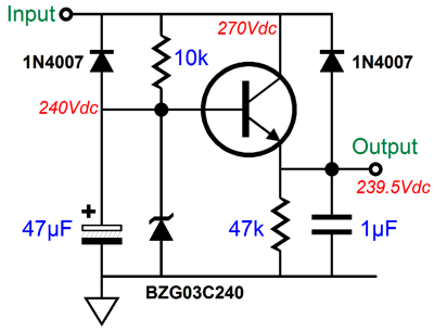
Using a PNP Transistor in Place of a Cathode Resistor The above circuit provides excellent ripple reduction (about -60dB worth), but it does not establish a fixed output voltage, as a change in the raw rectified B+ voltage results in a change in output voltage. Replacing the bottom voltage-divider resistor with a zener, however, will serve to establish a fixed DC output voltage. Note how we had to replace the 28k resistor with a 10k one. Why? The zener requires a threshold current to flow before it breaks at its stated voltage; the 28k would probably prove insufficient.
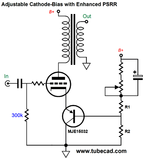
The lack of a fixed output voltage from a capacitance-multiplier circuit may actually prove more useful in an actual tube power amplifier than the fixed output voltage version. For example, if the wall voltage falls too much, then the zener will not break at its specified voltage. If the wall voltage climbs too high, the pass device may overheat. For example, a 10% increase in wall voltage may result in a 200% increase in emitter-to-collector voltage with a zener voltage reference, which against the same current draw will double the transistor’s heat dissipation. Whereas, with the two-resistor voltage divider capacitance-multiplier circuit, a 10% increase in B+ voltage will only results in a 10% increase in the transistor’s dissipation. The following schematic shows how an adjustable cathode-bias circuit could be made with a PNP transistor.
Move the potentiometer’s wiper up and the idle current falls, as we have effectively made the grid more negative relative to the cathode. Move the wiper down and we make the idle current increase. With little effort and expense, we can make a fancier version of this circuit.
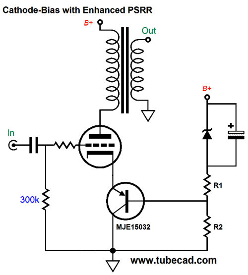
The diode is a safety device that allows the 1µF capacitor to safely discharge at the amplifier’s shutdown. The 10µF capacitor bypasses the PNP transistor at high frequencies. This circuit, however, neither establishes a constant-power nor a PSRR improvement. Adding a PSRR enhancing functionality is not all that hard, just some part reconfigurations, as the following schematic shows.
The potentiometer still sets the idle current and the two-resistor voltage divider (R1 & R2) feeds the PNP transistor’s base the required sampling of power-supply noise needed to create a ripple null in the single-ended amplifier’s output. In a nutshell, the triode cannot increase its current conduction in the presence of an increase in B+ voltage, as the 1/(mu + 1) increase in cathode voltage cancels the increased plate voltage, as the cathode functions in current anti-phase to the plate and grid. In other words, if we increase the cathode voltage, the triode’s current conduction will fall; whereas, if we increase either grid or plate voltage, the current increases. Resistor R1 must be mu times bigger than resistor R2. We could replace the top resistor and potentiometer with a high-voltage zener.
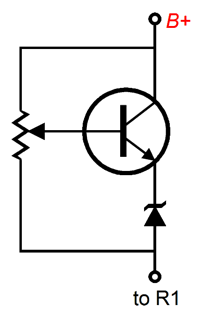
If you stop and think about it, you will realize that the above circuit results in a fairly constant-current idle current flow from the triode, in spite of variations in the wall voltage. How so? The zener always drops a fixed voltage, so any change in B+ voltage is directly transferred to the top of the two-resistor voltage divider. Thus, in the exact same way that the power-supply AC noise is cancelled by maintaining a fixed current flow, any change in the B+ voltage’s DC value is countered by a 1/(mu + 1) change in cathode voltage, which undoes the DC shift in B+ voltage. But, John, since we lost the potentiometer, we can no longer set the desired idle current. True, absolutely true. What we need is a variable zener. Fortunately, we can make such a device out of a few parts, which includes a low-voltage zener.
This circuit is a type of shunt regulator, which strives to present a fixed DC voltage to the NPN transistor’s base, which is only possible if the voltage drop across the circuit is fixed. An adjustable high-voltage zener, in other words. of course, we can and should strive to be a bit fancier.
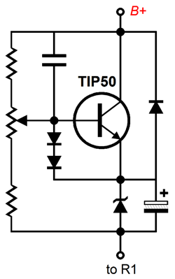
The diodes add safety by limiting the maximum base voltage swings relative to the emitter; the added two resistors limit the potentiometer's voltage-adjustment range; and the capacitor that attaches to the B+ relays AC signal to the base, while the zener-shunting capacitor lessens the zener noise. We can, of course, flip the circuit by using a PNP transistor instead.
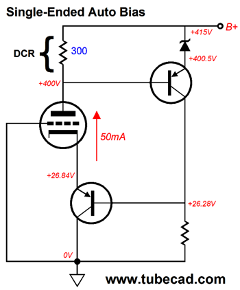
Adding the above circuit to the amplifier achieves two things: an adjustable idle current and a constant-current draw, but not a constant-power dissipation. To realize this last goal will require a means by which we can monitor changes in the wall voltage and a way to alter the idle current in response to those voltage changes.
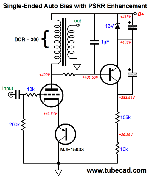
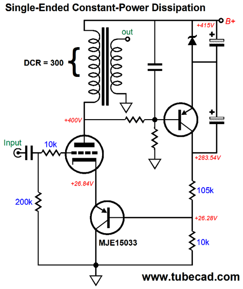
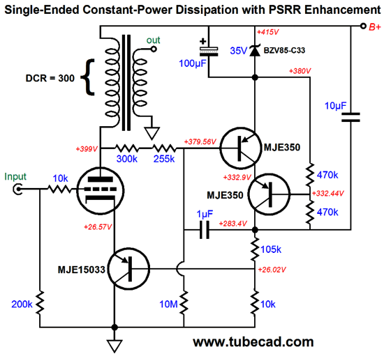
The above circuit uses the DCR (Direct-Current Resistance) of the output transformer’s primary as a current-sense resistor. As the voltage drop across this winding increases, the cathode voltage also increases, which lowers the output tube’s current conduction. Note how the PNP transistor's base voltage is slightly higher than the triode's plate voltage. This is due to the base drawing some current through the base resistor. The 1µF capacitor shunts away the AC signal from the plate. Perhaps that was too much, too soon for most readers. Let's forget about audio signals, transformers, and the PSRR enhancement and concentrate on the the auto-bias function.
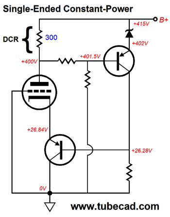
The theory of operation is simple enough: if the voltage drop across the primary's DCR is too great, then the top PNP transistor will increase its conduction, which will pull up the collector voltage, which in turn will raise the bottom PNP transistor's base voltage, which will cause the cathode voltage to increase, making the grid effectively even more negative than the cathode, causing the triode to conduct less, reducing both the current through the primary and the voltage drop across the primary. Now, all that is left is to add constant-power dissipation to the mix. Before examining the following schematic, pause and consider what might be needed. Our goal is to make the circuit aware of changes in the B+ voltage and then to compensate for those changes. It sound difficult, but the solution requires only one more resistor.
As the B+ increases, the idle current decreases, as the top PNP transistor's base must see a constant voltage from base to B+ voltage. Next, we add my signature Aikido-esque PSRR enhancement.
Now, we have finally arrived, as the output stage exhibits a constant-power dissipation. Since the top PNP transistor and zener are referenced to the B+ voltage, the transistor's base needs to know how far away ground potential is, a task that the added resistor performs. Think about it: if this added resistor attached to the B+ voltage instead, the base would never see a change in B+ voltage; but by terminating the resistor into ground, the transistor's base becomes aware of how much more positive it is to the ground and, thus, to changes in this voltage. One problem we face is that the highest-voltage PNP transistor that I know about is the MJE5852G, which can only withstand an emitter-to-collector voltage of 400V. The easy workaround is to cascode two PNP transistors.
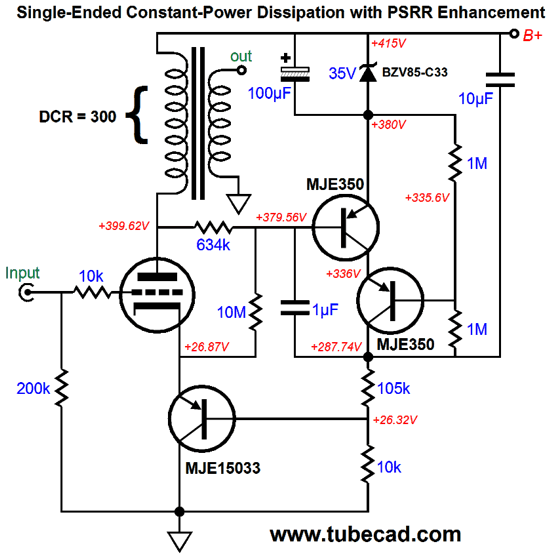
The two MJE350 PNP transistors can survive the 415V B+ voltage, as each device is rated for 300V. Note the 10µF capacitor, which shunts the high-voltage "zener" circuit. In SPICE simulations, I found that the following variation provided even better performance.
How does it differ? Note where the 10M resistor terminates, not to ground, but to the MJE15033's base. If you think about it, this makes sense, as the constant-power circuit needs to know more about what the actual cathode-to-plate voltage is for the output tube than what the B+ voltage is. Okay, since this seems to be our end point, let's apply one last burst of finishing touches.
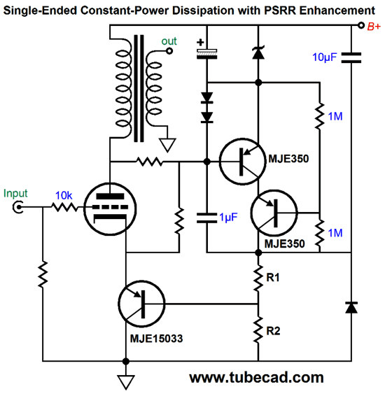
The part values and voltages have stripped away, purposely. The topology is universal. Output tubes are not limited to 300B and EL34 types, as a 2A3 or 6L6 (triode-connected) or EL84 (ditto) or 845 could be used. In the case of a 211 or 845 or any other high-voltage triode, more MJE350 transistors would have to be cascoded. And, of course, this is just a naked output stage, albeit an elaborate one. nonetheless, an input (and possibly a driver) stage will be needed. Remember my rule: when designing a power amplifier, work from the end to the front.
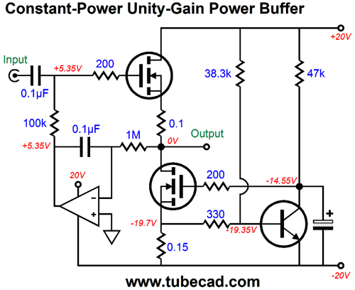
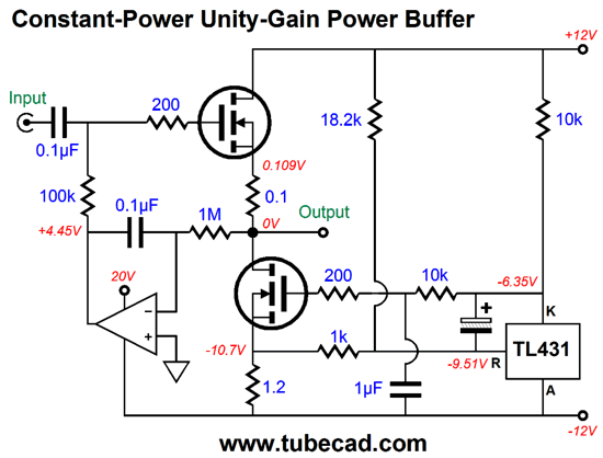
Constant-Power Unity-Gain Power Buffer
The MOSFETs are IRF230 types, but any robust MOSFET could be used, such as the IRFP240PBF, if adequately heatsinked. (A huge heatsink would be required.) Note the voltage drops across the 330-ohm and 38.3k resistors; then note how they relate to the resistor values.
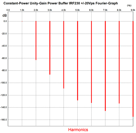
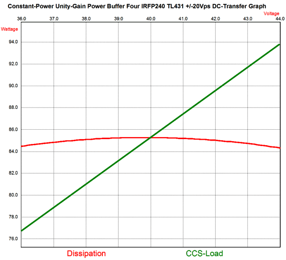
The green plotline shows how a constant-current source load would perform with a varying wall voltage. By the way, the dissipation is for the entire output stage and the voltage is the entire voltage differential between power-supply rails. How well does this power buffer perform in terms of distortion? Here is the SPICE graph for 1W at 1kHz into an 8-ohm load.
At full output (16W), the distortion goes up, but the same single-ended structure remains. I like this circuit a great deal, as we do not ask too much from the MOSFET, as it only needs to provide gobs of current, not voltage gain. Gain, about 16x or +24dB, we can easily get from tubes. Indeed, an Aikido line stage amplifier based on 6DJ8 tubes would work perfectly, as it would deliver a gain of +24dB.
A relatively low B+ voltage of 150Vdc could be used with the 6DJ8 tubes. I know that many imagine that I would include the above Aikido within the power buffer chassis. I wouldn't. Think about it: why would we need two line-stage amplifiers, one cascading after another, one external to the power buffer, one within the power buffer. We wouldn't, as we can use just one line-stage amplifier external to the power buffer that puts out an extra-hot output signal, a big, juicy signal large enough to drive the power buffer to full output. Of course, high voltage gain is not enough, as the MOSFET gate presents a good amount of input capacitance. To drive this capacitance at high frequencies requires current. Thus, a high idle current should be run in the Aikido's output stage, say at least 10mA. Another thought is that since I complained before about transistors exhibiting too great base-to-emitter voltage shifts with changing temperature, why I am I now using one? Well, we do not have to, as we could use a TL431 instead.
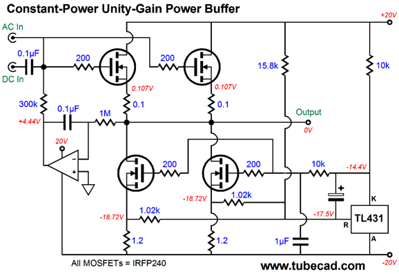
Note the lower idle current and power-supply rail voltages. Why? I worry about the two MOSFETs becoming too hot. With these values, we could expect 4W of output into 8-ohm loads. If you own high-efficiency speakers or need a tweeter amplifier, the 4W could prove to be plenty. On the other hand, we could go back to the +/-20V rails and 16W of output by doubling up on the MOSFETs.
Note that only one TL431 was used. Also note that two inputs are offered. The AC-in input would be used when the line-stage amplifier uses a coupling capacitor at its output; the DC-in input, when the line-stage amplifier is DC coupled at its output. The entire output stage dissipates about 85W at idle per channel, so a heatsink with no more than 0.4C/W thermal resistance would be required per channel, as such a heatsink would keep the heatsink temperature just below 60C and the MOSFET junction temperature at 90C, assuming an ambient temperature of 25C.
As the graph above reveals, the constant-power circuit out performs the normal constant-current-source loading.
Next Time
User Guides for GlassWare Software Since I am still getting e-mail asking how to buy these GlassWare software programs:
For those of you who still have old computers running Windows XP (32-bit) or any other Windows 32-bit OS, I have setup the download availability of my old old standards: Tube CAD, SE Amp CAD, and Audio Gadgets. The downloads are at the GlassWare-Yahoo store and the price is only $9.95 for each program. http://glass-ware.stores.yahoo.net/adsoffromgla.html So many have asked that I had to do it. WARNING: THESE THREE PROGRAMS WILL NOT RUN UNDER VISTA 64-Bit or WINDOWS 7 & 8 or any other 64-bit OS. One day, I do plan on remaking all of these programs into 64-bit versions, but it will be a huge ordeal, as programming requires vast chunks of noise-free time, something very rare with children running about. Ideally, I would love to come out with versions that run on iPads and Android-OS tablets.
//JRB |
Kit User Guide PDFs
And
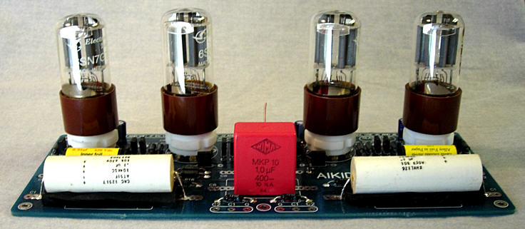
High-quality, double-sided, extra thick, 2-oz traces, plated-through holes, dual sets of resistor pads and pads for two coupling capacitors. Stereo and mono, octal and 9-pin printed circuit boards available.
Designed by John Broskie & Made in USA Aikido PCBs for as little as $24 http://glass-ware.stores.yahoo.net/
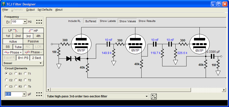
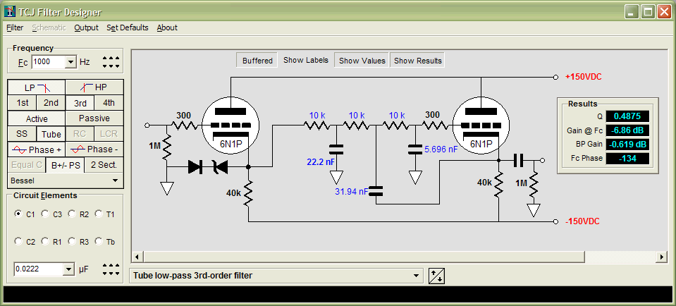
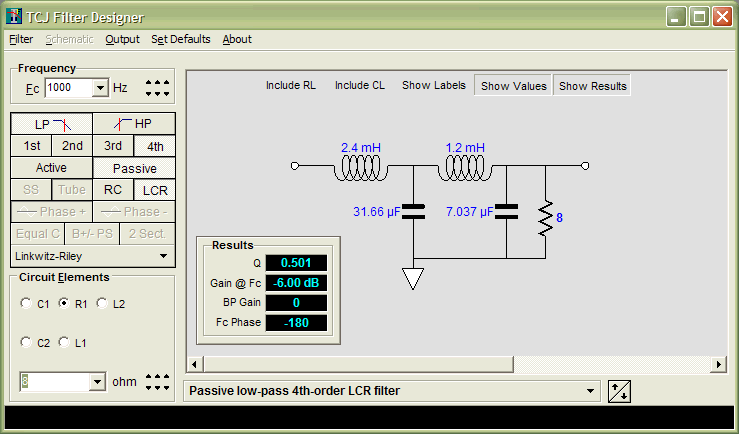
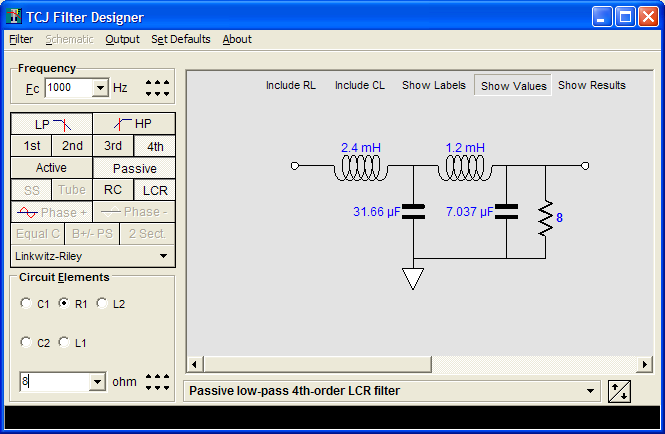
The Tube CAD Journal's first companion program, TCJ Filter Design lets you design a filter or crossover (passive, OpAmp or tube) without having to check out thick textbooks from the library and without having to breakout the scientific calculator. This program's goal is to provide a quick and easy display not only of the frequency response, but also of the resistor and capacitor values for a passive and active filters and crossovers. TCJ Filter Design is easy to use, but not lightweight, holding over 60 different filter topologies and up to four filter alignments: While the program's main concern is active filters, solid-state and tube, it also does passive filters. In fact, it can be used to calculate passive crossovers for use with speakers by entering 8 ohms as the terminating resistance. Click on the image below to see the full screen capture.
Tube crossovers are a major part of this program; both buffered and un-buffered tube based filters along with mono-polar and bipolar power supply topologies are covered. Available on a CD-ROM and a downloadable version (4 Megabytes). |
||


| www.tubecad.com Copyright © 1999-2016 GlassWare All Rights Reserved |