| John Broskie's Guide to Tube Circuit Analysis & Design |
25 June 2016 Post 385
Exploiting Switcher Power Supplies
Recently, I was thinking about how a switcher power supply could be used to make a single-ended power amplifier—solid-state of course. Single-end amplifiers cannot help but run in strict class-A, which means that they run hot. Finger-burning hot. I love my car engine analogy from post 347, and again in post 361, so I will quote myself:
Moreover, the power transformer within the class-A power amplifier gets hot, due to core losses, eddy currents, and the wire's resistance. We cannot alter the class-A generated heat, but we can offload the power supply heat to a switcher power supply, particularly if the switcher is located external to the amplifier's chassis. In addition, by using an external power supply, we free up a lot of space within the enclosure, which is always in short supply. If nothing else, we could fill the freed-up space with extra heatsinks. My first thought was that the inductor-loaded design from post 361 would be a good idea.
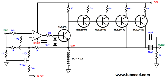
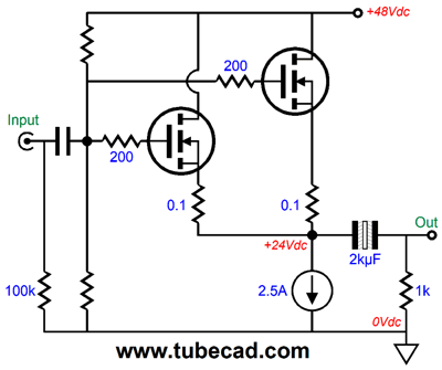
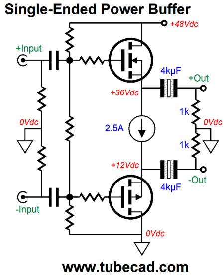
One problem with this circuit is that requires a bipolar power supply, which are sold in the desktop switcher package. The thing is that we only need a few milliamps of current from the negative power-supply rail, but 4A of current from the positive rail (2A at idle and 4A at peak output). Besides, I wanted to use a monopolar switcher power supply, preferably from my existing stash of high-current switcher power supplies. My next thought was why make a power amplifier, when a power buffer would work. Well, it would work, if a hot tube line-stage amplifier were used to drive it. A good tube-based line stage should easily be able to put out 20Vof peak voltage swing. For example, a 12AT7-based Aikido line stage would deliver a gain of 30 and easily swing 20Vpk of clean output signal. Now, 20Vpk into an 8-ohm load equals 25W of power. The math is simple: square the peak voltage swing and divide it by twice the load impedance, or put mathematically, 20²/16 = 25 watts. (If we know the peak current swing, on the other hand, we use I² x R/2 = Watts.) Here is an example of a single-ended power buffer.
The gate-stopper resistor should be a low-inductance type, such as a carbon-composition or bulk-foil resistor. The output coupling capacitor could/should be a non-polarized type, which seldom are made bigger than 470µF in size, so several would have to be put in parallel; this is actually a good thing, as it lowers the ESL (effective series inductance) and helps keep the capacitors cool, due to increased surface area. The constant current source can be made up from a power MOSFET, as shown below.
The single power MOSFET, used as the source follower in the power buffer, can be any big, high-wattage, N-Channel, power MOSFET, preferably in the TO-247-3 package. Since we know the idle current is 2.5A and we know that the buffer MOSFET sees half of the 48V power supply voltage, we also know that the MOSFET's dissipation at idle will be 60W. This is crazy hot a solid-state device. Even a modern high-wattage device, such as the 450W STW40N95DK5 would have a hard time surviving Here are its specifications from the Mouser website.
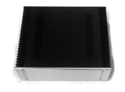
The most important specification, well at least to us in this application, is missing from this list. It is its thermal resistance junction-case (Rthj-case), which for this device is an amazingly low 0.28 °C/W. Still, the math isn't great. Assuming an insulator thermal resistance of 0.7 °C/W and a heatsink resistance of 05 °C/W and an ambient temperature of 25 °C and 60W of dissipation at idle, we get a junction temperature of 114 °C and a heatsink temperature of 55 °C. Mind you, a thermal resistance of only 0.5 °C/W means a huge heatsink. And it gets worse, as the constant-current source will also dissipate 60W at idle. Actually, I was thinking of a mono-block power buffer in one of those amplifier enclosures from China, such as the following.
I would place the buffer MOSFET on one heatsink and the constant-current-source MOSFET on the other heatsink. Still, 120W of heat is tough to get rid of, without resorting to forced-air cooling. In addition, the heatsink might be rated for only 0.5 °C/W, but that might mean along its length, not for one device placed at its center. Now, if we used two 150W MOSFETs, for example the IRFP240, which cost only $2 each, in place of one 450W MOSFET, the math works out much better, in spite of the IRFP240's higher thermal resistance junction-case of 0.83°C/W, as each MOSFET's junction temperature would be only 101 °C.
The MOSFET would have to be matched, but new-production MOSFETs come close close to matched out of the shipping tube these days. Or we could give each MOSFET its own constant-current source.
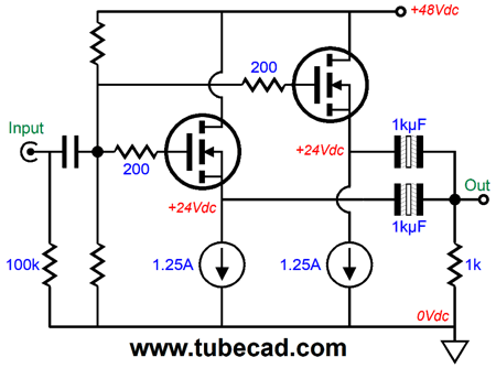
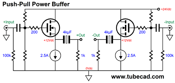
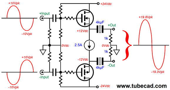
I prefer this arrangement. What if we were using a balanced tube line-stage amplifier instead? Well, we know that the peak signal voltage swing would halve, from 24Vpk down to +/-12Vpk. But then we could also halve the B+ voltage, from +48Vdc down to 24Vdc, but at the cost of twice the current flow. No free lunches in electronics.
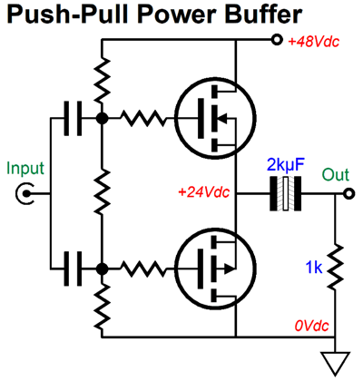
Note that this is a push-pull power buffer, not a single-ended one, although each buffer MOSFET is operated in a single-ended fashion. The all-important distortion characteristics will be push-pull in structure. Indeed, the constant-current source only buy us auto-bias of the buffer MOSFETs. So, how would we build a single-ended, balanced power buffer?
Single-Ended Balanced Power Buffer
Wait a minute, John, this just like any MOSFET-based push-pull output stage; there's nothing single-ended about it. No. You are confusing it for this this, which it is not.
They may make look similar, but they differ in one key way: current phase. The balanced-input version operates both N- and P-channel MOSFET in the same current phase, so both increase and decrease current conduction in phase. In contrast, the above push-pull buffer accepts a single-ended input signal, so the two MOSFETs operate in anti-current-phase to each other, so as one increases current conduction, the other decreases its conduction. Does this make a difference? Big time. The above buffer will produce a symmetrical output signal, whereas the single-ended version won't.
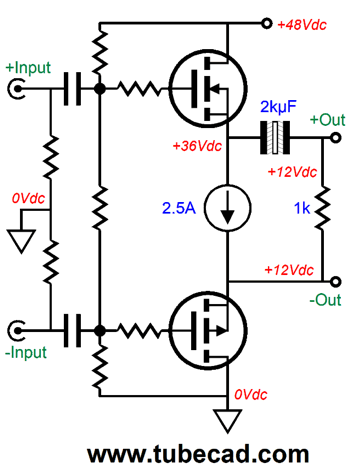
MOSFETs are not perfectly linear; no electronic device is. They are easier to turn on than to turn off, so positive input signal swings will result in a slightly bigger output voltage swing than negative input signal swings. The result is a strong 2nd harmonic component. In the above schematic, we see that on the first half of the input sinewave, both MOSFETs increase their conduction, pulling the two outputs apart, on the second half, they both decrease their conduction, allowing the constant-current source to pull the two MOSFET sources together. Note the 4kµF output coupling capacitors. Why double the previous value? Each MOSFET effectively sees a 4-ohm load, not an 8-ohm load; thus, we must double the output coupling capacitor value. A workaround is to use only one output coupling capacitor.
Now, we can use the same 2kµF value, which allows output down to 10Hz. We incur, however, a 12Vdc voltage offset on both output terminals. The speaker is safe, as it sees 0V of voltage differential at idle, but we should avoid shorting either output terminal to the chassis. As I looked at the above schematic, I was reminded of a circuit from 43 years ago.
A. M. Sandman's Error Takeoff Distortion Reduction
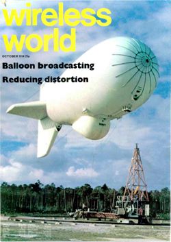
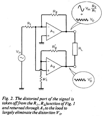
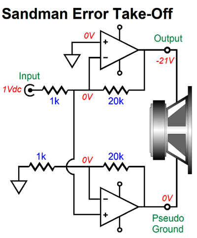
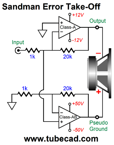
Here is his illustration from the Wireless World magazine October issue of 1974.
The smaller squiggly lines represent distortion from amplifier A1, which amplifier A2 presents at its output. Amplifier A2 has but one job: to act as a pseudo ground and reproduce the top amplifier's distortion product in phase and in equal magnitude. If amplifier A1 were perfect, then amplifier A2 would serve as a virtual ground. Let's fill in some part values.
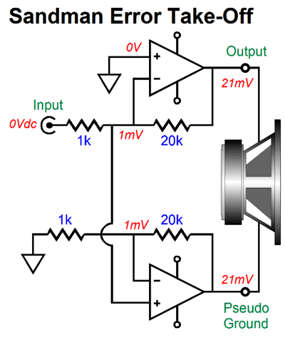
With no distortion from the top amplifier, we get the following results.
The bottom amplifier has no input signal to amplify, as the top amplifier didn't produce any. Let's say that it does, for example a small DC offset at its output counts as a distortion, although not a harmonic distortion.
The important feature is that the top amplifier functions as an inverting amplifier, while the bottom amplifier functions as a non-inverting amplifier. The top amplifier's gain is 20, but the bottom amplifier's gain is 21. This is important, as the bottom amplifier's positive input sees 1/21 of the top amplifier's distortion and the loudspeaker must see an equal amount of distortion at each terminal for it to ignore the distortion. Since the bottom amplifier acts as a pseudo ground, it can run on much lower power-supply-rail voltages.
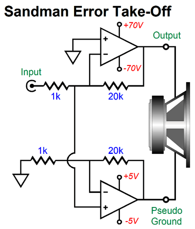
There is one case, however, where the above use of dissimilar rail voltages would not work. Say that the top amplifier fails to put out any signal whatsoever, i. e. zero volts. Well, then the bottom amplifier would see 20/21 amount of the top amplifier's input signal, due to the 1k and 20k resistors forming a voltage divider. And the bottom amplifier's gain of 21 against 20/21 equals 20, which was what the top amplifier was supposed to produce; and with no phase inversion, as the speaker negative terminal attaches to the top amplifier's output. In other words, we still get the desired output—but only if the bottom amplifier can make the required output voltage swings. One possible arrangement is the one I made in post 284, which showed the following schematic.
The amplifier that had been on the bottom is now on the right. It runs in class-G, which means that at idle its power-supply-rail voltages area low +/-12V, but when needed, the rail voltages can climb to +/-27V. Perhaps, this is the wrong way to go. Perhaps, we should reverse the voltages, so the the pseudo-ground amplifier gets the bigger rail voltages.
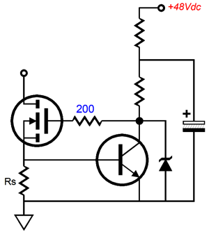
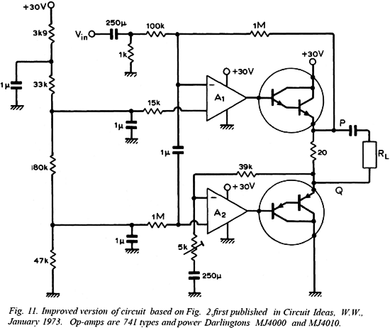
When the top amplifier runs out of voltage and begins to clip, the bottom amplifier begins to swing in earnest, allowing much bigger output voltages to develop. Of course, the bottom amplifier will not run as clean, but then the ear becomes less sensitive as the music volume goes up. Returning to switcher power supplies, here is the 43 year-old schematic that I recalled when looking at the balanced-input single-ended amplifier schematic. (Amazing how 43 years doesn't sound that long ago, considering that the Sgt. Pepper's Lonely Hearts Club Band album is 50 years old. has popular music really surpassed it? Cough, cough. But in electronics, 43 years is equivalent to a century in another endeavor.)
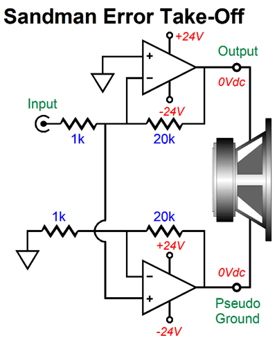
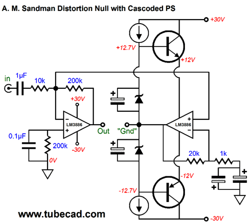
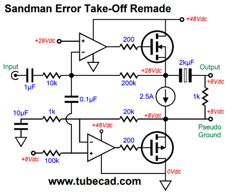
Note how Darlington output transistors are used, not MOSFETs; also note how a 20-ohm load resistor is used in place of the constant-current source; most importantly, note how a mono-polar power supply is used. Let's remake this venerable design.
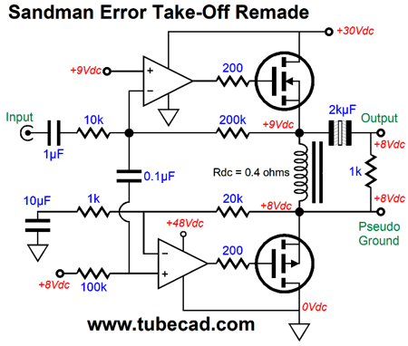
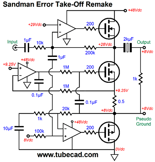
Gone are the Darlington transistors; gone is the 20-ohm load resistor. The three-resistor voltage divider required to create the 8V and 29V reference voltages is not shown, but it is easy to imagine. Can you imagine removing the constant-current source. It's possible, just replace it with an inductor.
The inductor acts like a compliant constant-current source and only displaces 1V at idle, due to its 0.4-ohms Rdc and the 2.5A idle current flow. Note how the B+ voltage only fell to 30Vdc, not 24Vdc. The MOSFETs limit the maximum output swing due to their relatively high turn-on voltage. Thus, even with a rail-to-rail OpAmp, the top MOSFET's source can only get to within 5 volts of the B+ voltage. In other words, you can only expect a +/-16Vpk voltage swing from the output, which equals 16W into 8-ohm loads. If we stick to the constant-current source version, then we have to come up with a constant-current source design that would work with the pseudo ground. Here is one possibility.
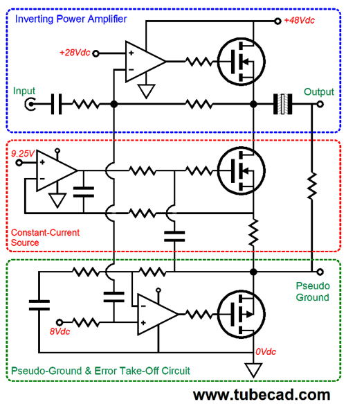
The design requires a third OpAmp and MOSFET. Here is the conceptual overview of the circuit.
The center OpAmp strives to maintain a fixed 1.25v voltage drop across the 0.5-ohm resistor. As the music plays, the bottom OpAmp sees the top amplifier's distortion output and it delivers the same amount of distortion to the pseudo-ground output, which means that a small signal will appear at this output. The constant-current source in the circuit middle does not "see" this signal, as its integrator time constant is too large. In other words, the center OpAmp only responds to sub-sonic signals. The center MOSFET, nonetheless, sees the same fixed gate-to-source voltage because of the 0.1µF capacitor at its gate-stopper resistor. The more I looked at this circuit, however, the less I liked the complexity of it. Why couldn't the constant-current source portion do the error take-off function, so the pseudo-ground portion could be eliminated?
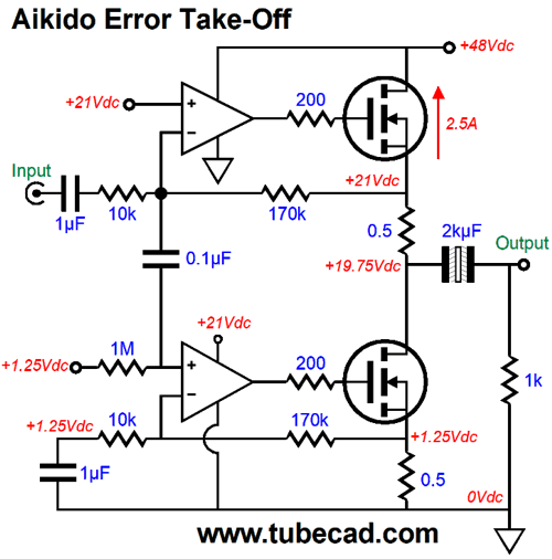
Aikido Error Take-Off
The input stage is a grounded-cathode amplifier with an active plate load. The cathode follower is also loaded by an active load, the triode below it. This bottom triode sees only the amplifier's distortion product at its grid, so it amplifies and inverts the distortion, creating a small reduction in distortion from the amplifier's output. The problem was that the bottom triode offered very limited transconductance, particularly with the unbypassed cathode resistor, so it could not do much distortion erasing. The following design does not suffer from this problem, as the bottom OpAmp and MOSFET present a screaming transconductance.
If the amplifier's output presents zero distortion, the bottom OpAmp and MOSFET function as a simple constant-current source. If the amplifier does distort, the bottom OpAmp sees the distortion as its input signal and it amplifies it and imposes atop the bottom 0.5-ohm source resistor, which creates a countervailing current variation that nulls the distortion at the output. The penalty we pay is an output impedance of 0.5 ohms, which results in a damping factor of just 16 with an 8-ohm load. Still, most tube-based single-ended amplifier run output impedances two to ten times greater. Note that the bottom OpAmp gets a 21V power-supply rail voltage, while the top OpAmp gets the full 48V, which is a huge voltage differential for an OpAmp. We can use different OpAmps. The top must be a high-voltage type, such as the OPA454 (which can withstand a 100V differential between its power supply pins) or OPA604 (48V). The bottom OpAmp, in contrast, can be just about any high-performance OpAmp, such as the AD797 or LT1115 or OPA1611 or OPA2107. Okay, I better call it quits now, before my fingers fall off. Expect part two next time.
//JRB
Special Thanks If you have been reading my posts, you know that my lifetime goal is reaching post number one thousand. I have 615 more to go. I should easily be able to hit post 400 this year. My second goal is to gather 1,000 patrons. I have 959 patrons to go. If you enjoyed reading this post from me for the last 18 years, then you might consider becoming one of my patrons at Patreon.com.
//JRB
User Guides for GlassWare Software Since I am still getting e-mail asking how to buy these GlassWare software programs:
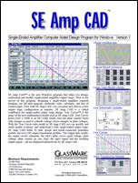
For those of you who still have old computers running Windows XP (32-bit) or any other Windows 32-bit OS, I have setup the download availability of my old old standards: Tube CAD, SE Amp CAD, and Audio Gadgets. The downloads are at the GlassWare-Yahoo store and the price is only $9.95 for each program. http://glass-ware.stores.yahoo.net/adsoffromgla.html So many have asked that I had to do it. WARNING: THESE THREE PROGRAMS WILL NOT RUN UNDER VISTA 64-Bit or WINDOWS 7 & 8 or any other 64-bit OS. One day, I do plan on remaking all of these programs into 64-bit versions, but it will be a huge ordeal, as programming requires vast chunks of noise-free time, something very rare with children running about. Ideally, I would love to come out with versions that run on iPads and Android-OS tablets.
//JRB |
Kit User Guide PDFs
And
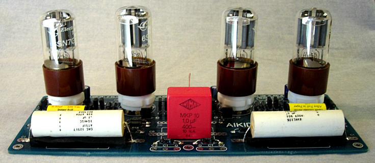
High-quality, double-sided, extra thick, 2-oz traces, plated-through holes, dual sets of resistor pads and pads for two coupling capacitors. Stereo and mono, octal and 9-pin printed circuit boards available.
Designed by John Broskie & Made in USA Aikido PCBs for as little as $24 http://glass-ware.stores.yahoo.net/
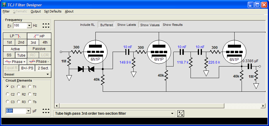
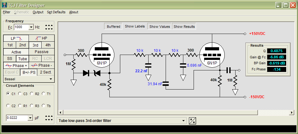
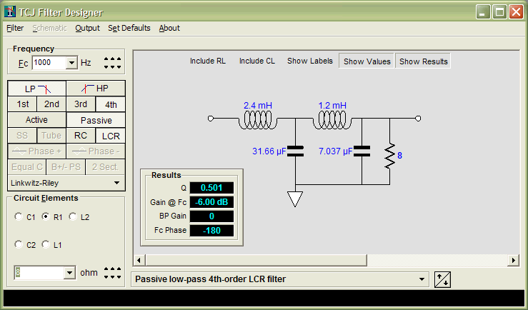
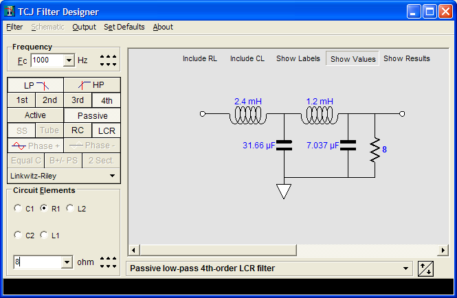
The Tube CAD Journal's first companion program, TCJ Filter Design lets you design a filter or crossover (passive, OpAmp or tube) without having to check out thick textbooks from the library and without having to breakout the scientific calculator. This program's goal is to provide a quick and easy display not only of the frequency response, but also of the resistor and capacitor values for a passive and active filters and crossovers. TCJ Filter Design is easy to use, but not lightweight, holding over 60 different filter topologies and up to four filter alignments: While the program's main concern is active filters, solid-state and tube, it also does passive filters. In fact, it can be used to calculate passive crossovers for use with speakers by entering 8 ohms as the terminating resistance. Click on the image below to see the full screen capture.
Tube crossovers are a major part of this program; both buffered and un-buffered tube based filters along with mono-polar and bipolar power supply topologies are covered. Available on a CD-ROM and a downloadable version (4 Megabytes). |
||||||||||||||||||||||||||||||||


| www.tubecad.com Copyright © 1999-2017 GlassWare All Rights Reserved |