| John Broskie's Guide to Tube Circuit Analysis & Design |
22 April 2018 Post Number 421
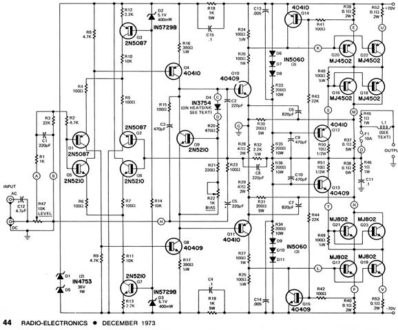
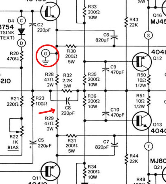
Errata Electronica Alas, much like spotting your own grammatical mistakes, spotting your own schematic typos is difficult. I spot them all the time, while reading books, magazines, and webpages—but then they weren't my schematics. A reader sent me the following schematic, which holds one huge circuit typo. It took me less than 30 seconds to spot it. Time yourself.*
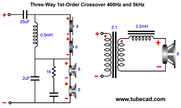
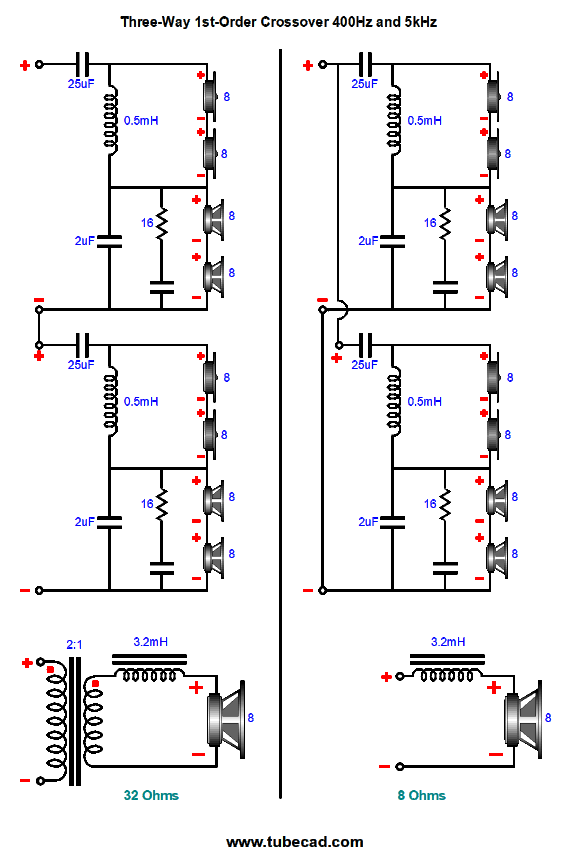
A few days ago, while drinking my morning coffee, I was going over my last post, when I found a schematic typo. The schematic held a crossover for making a 32-ohm/8-ohm loudspeaker. I had got all the values right, save for the big capacitor, which I had made twice as big as it should have been, as I couldn't shake an 8-ohm load from my mind. Here is the corrected schematic.
In fact, I not only replaced the original, I added a new schematic to show how the complete crossover would be set up.
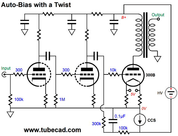
A week prior to that discovery, I had found a schematic typo in post 409. I had been quite pleased with the post up until I came across the following schematic.
Shown above, is the corrected schematic, but the original failed to include the decoupling capacitor next to the red "B+" marking. I didn't spot it at first, but I felt queasy, almost as if I were suffering from a bout of vertigo as I looked at the schematic. (I understand that something similar happens to chess masters when they are shown a chess position where either black or white's two bishops are on the same color. They first feel disoriented, dizzy, and then they find the problem.) Without this capacitor, the circuit makes no sense, as very little amplification would obtain. With a big capacitor in place, the constant-current source will both auto-bias up the 300B output tube and shield the amplifier from the power-supply noise, much as a huge inductor would. The price we pay, a small price at that, is that each channel must get its own floating high-voltage power supply. This is a radically different approach to the usual heavy emphasis on the smoothing the B+ voltage, as this alternate approach smooths the ground. It works because the single-ended output stage runs in strict, not make-believe, class-A, so the amplifier draws a constant average current. If we replace the single-ended output stage with a push-pull, class-A output stage, this same trick could be employed.
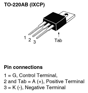
An added advantage to this setup is that we could use an IXCP 10M45S or 10M90S constant-current source and not use an isolation washer between its TO-220 tab and the heatsink, as its tab connects to its anode and its anode will be at exactly ground potential in this circuit. (We would still use some thermal grease.) And if we are truly sneaky, we could implement a slow-turn-on constant-current source, which would slowly develop the full B+ voltage.
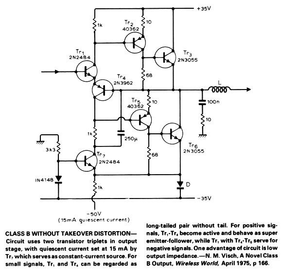
Visch Output Stage Well, I could not find in San Jose a store that sold the Wireless World magazine, but the libraries carried it. Yet, all the supermarkets sold Popular Electronics and Radio Electronics magazines, along with Audio, High Fidelity, and Stereo Review magazines. Those were the days, as Audio often held schematics. (You could readily buy Wireless World in San Francisco and Berkeley and Los Angeles.) Returning to Mr. Visch and his output stage, I remember being baffled by his schematic. Every time that I thought that I had grokked it in its entirety, I ran into the diode marked "D" in the following schematic. Everything made sense but that diode. Why was it there? What could it possibly do?
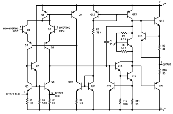
By the way, I scanned the schematic above from John Marcus' book, Popular Circuits Ready Reference. His nutshell description sums the circuit up nicely. I will just add a few more details. Transistor Tr7 is configured as a constant-current source at idle and at low output signal levels. But once bigger output swings occur, transistor Tr6 draws enough current to forward bias the "D" diode and Tr7-based constant-current source switches off, as its base-to-emitter voltage approaches zero volts. At idle, transistor Tr7's 1k emitter resistor sees a current flow of 15mA, which is split up by the bastode input stage and output stage. If the output transistors draw too much of the 15mA of current flow, the bastode resistors become current starved and the output stage must draw less current, as transistor Tr2 sees too little base-to-emitter voltage. If the output transistors draw too little current, however, the surplus ciurrent must flow through the bastode's two 1k resistors, which then see a much larger voltage drop, and which would, in turn, force the output transistors to increase their conduction. In other words, the two stages must fall into an equilibrium. All in all, a brilliant design—including the dang diode. Effectively, this diode is only in the circuit when it needs to be. Brilliant. I was just about to say that this was the first occurrence of the bastode topology I had seen, but my leaky memory came to the rescue. Back in 1968, the famous LM741 integrated circuit was designed at Fairchild Semiconductor by David Fullagar.
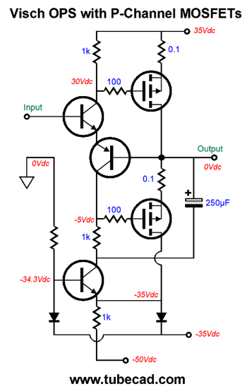
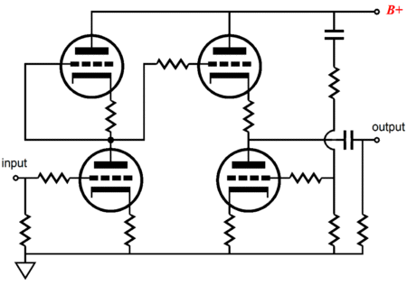
As you can see in the schematic above, transistors Q1 & Q3 and Q2 & Q4 define bastode cascodes. Returning to Visch's circuit, the bastode stage offers gobs of gain, which wraps around the output stage in a short, tight negative-feedback loop. This localized feedback results in less crossover distortion (Visch called it "takeover distortion") and the noted low output impedance. The key device in this setup is the 250µF capacitor, as it ensures equal drive signals to the two sets of output transistors. This capacitor is not a bootstrap capacitor, which magnifies impedances, but a signal subtracting capacitor. Let's replace the output transistors with two P-channel MOSFETs (which are functionally similar the the compound transistors) to make the operation clearer.
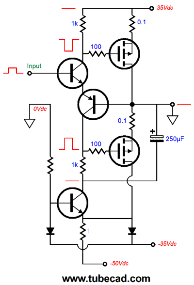
The 250µF capacitor relays 100% of the audio frequencies to the bottom of the 1k resistor, so both MOSFETs see the same amount of gate-to-source drive signal, in spite of the bottom MOSFET's source swinging up and down with the output voltage swings. Still not seeing it? Okay, then imagine that the output is shorted to ground.
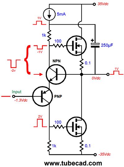
Let's then apply a single 1V positive pulse to the input and also assume that the bastode gain stage only realizes a gain of 2. Since both 1k resistors see the same current flow and since both are fixed at one end, they both develop the same 2V pulse, but in anti-phase relative the MOSFET gates. Thus, the top MOSFET greatly increases its current conduction, while the bottom MOSFET greatly reduces its. Push-pull operation, equal push-pull operation, obtains. What happens when the output is allowed to swing up and down?
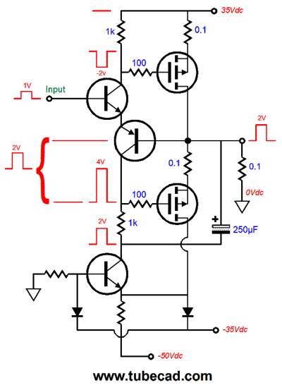
The same 1V input pulse is applied and the output swings up by 2V, yet each MOSFET sees the same 2V drive signal. Assuming MOSFETs with near infinite transconductance, the 0.1-ohm source resistors effectively limit their transconductance to 10A/V, so the 2V drive signal results in a turned off bottom MOSFET and a top MOSFET conducting 20A of current. which into the 0.1-ohm load results in a 2V positive pulse at the output. Now, let's see what happens when we ground the input and apply the pulse to the output.
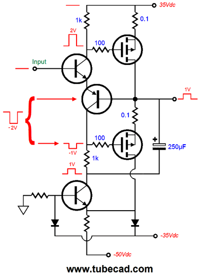
The positive pulse is amplified by two and presented to the top MOSFET's gate in phase, which is large enough to turn off this MOSFET. The bottom 1k resistor sees the decrease in current flow and experiences the same -2V voltage drop across its leads, but the 250µF capacitor pulls its bottom lead up by 1V, so relative to ground, only a -1V pulse develops. But relative to the bottom MOSFET, the pulse is equal to -2V, as its source resistor terminates into the +1V pulse. Note how the bottom MOSFET's increased current conduction works to fight the imposition of the positive pulse at the output. We would then conclude that since a 1V pulse prompted a 20A current flow, the output impedance is equal to 1/20 or 0.05 ohms. (We are ignoring the idle current, which we assume to be tiny.) And 20A of current flow occurs well after the output stage has departed from its class-A window of operation. On the other hand, while both MOSFETs are still conducting, the output impedance would equal half that previous value, being 0.025 ohms. This is the result of gm doubling, where both output devices are adding their transconductances together in the class-A window of current flow, but only in that window of operation. Now it's time to replace the P-channel MOSFETs with N-channel MOSFETs, which is a steppingstone to vacuum tubes.
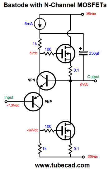
The top MOSFET now gets the 250µF capacitor treatment and the PNP transistor becomes the input transistor, while the NPN transistor becomes the inverting input. The 5mA constant-current source sets the voltage drop across the two 1k resistors, which in turn sets the idle current flow through the MOSFETs. An input signal applied to the PNP transistor's base will prompt the output to follow, making this a unity-gain power buffer (as were all the previous circuits). If the 1V positive pulse is forced upon the output, the following results.
The bastode input stage develops its gain of 2 once again, so the bottom 1k resistor sees a 2V pulse, which causes the bottom MOSFET to increase its current conductance, which will buck the positive pulse at the output, as the this MOSFET will strive to pull the output back to zero volts. In contrast, the top MOSFET sees the 1V pulse at the bottom of its source resistor and a -1V pulse at its gate, which will shut down its current conductance. So once again, we see a 20A current flow and the same output impedance of 0.05 ohms. The next step is to replace the MOSFETs with triodes.
6AS7-Based Bastode Buffer
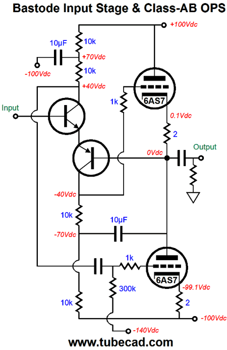
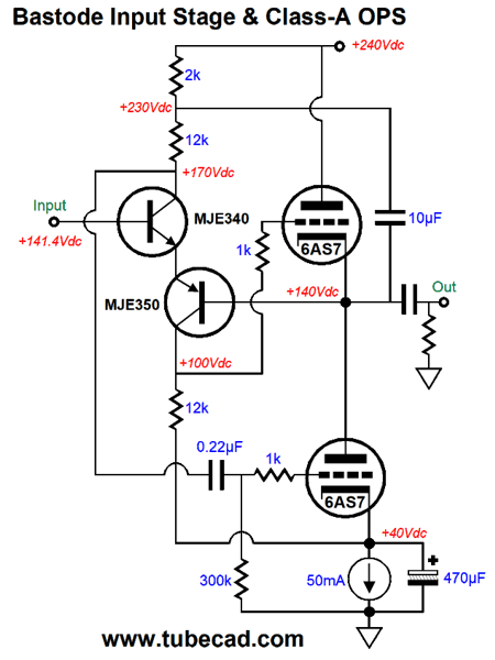
The first step to making the transition to triodes is to increase the bipolar power-supply voltage to +/-100Vdc and to add an internal coupling capacitor for the bottom 6AS7 triode.
Note how the top 6AS7 triode is DC coupled to the PNP transistor's collector, but the bottom 6AS7 triode's grid is AC coupled to the NPN transistor's collector. Also note the -140V negative bias voltage that is needed for the bottom 6AS7 triode. The 250µF capacitor has been replaced by just a 10µF due to the two 1k collector resistors being replaced by 10k resistors. The added 10µF capacitor at the top of the circuit is essential as is its termination into the negative power-supply rail, not ground. Why? Well, other than it being one of my signature moves, this arrangement ensures that 100% of the negative power-supply rail noise appears at the bottom triode's grid. If this capacitor terminated into ground, then the bottom triode would "see" 100% of the negative power-supply rail noise, which the above setup had made invisible to its grid and cathode. Creating an extra negative power-supply rail voltage of -200V is not difficult. But for those who eschew negative power-supply rails altogether, the following design —which uses a mono-polar power supply and cathode biasing—will prove more desirable.
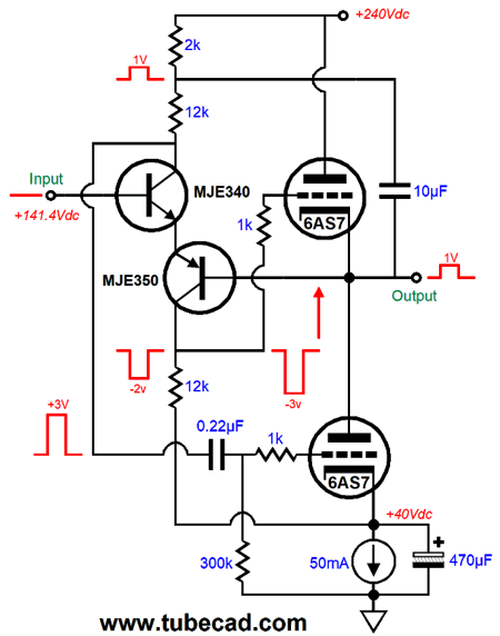
The B+ voltage had to be increased to 240V to absorb the 40V lost across the constant-current source, which auto-biases the triodes. Nonetheless, each triode still sees a cathode-to-plate voltage of 100V and draws the same 50mA. The biggest change, however, is where the 10µF capacitor terminates. This time, it's at the top of the top 12k collector resistor. Placed at the top, this capacitor becomes a signal adder, not a signal subtractor. To see how this setup works, let's apply the 1V positive pulse to the output, with the input grounded.
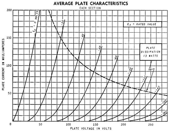
Assuming the same amazingly-low gain of just two from the bastode input stage, the 1V pulse prompts a 2V decrease in voltage drop across both 12k resistors. Thus, the top triode sees its cathode rise by 1V and its grid voltage drop by -2V, with net total of -3V change in cathode-to-plate voltage. At the same time, the bottom triode sees the relayed 1V pulse and 2V pulse created by the bastode stage add together to a net +3V pulse at its grid. Balance. Each triode equally responds to the externally applied pulse. At 100V and 50mA, the 6AS7 exhibits a transconductance of about 4.25mA/V, so both triodes would add up to 8.5mA/V, which means that the change in current flow would equal 8.5mA against 3V or 25.5mA, which implies an output impedance of about 40 ohms. In actual use, however, the bastode input stage will deliver a vastly higher gain, with a resulting vastly lower output impedance. We could, however, rearrange the circuit to the way it was originally shown in the bipolar-power-supply version, where the 10µF capacitor appeared at the bottom, rather than at the top.
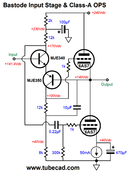
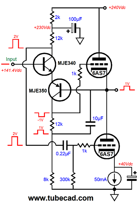
This arrangement is equally balanced, as both triodes work equally and see equal cathode-to-grid drive signals, albeit in anti-phase. Once again, let's apply the 1V positive pulse to the output, with the input grounded.
Both 12k collector resistors see the same 2V voltage drop, but the two triodes only see a 2V countering drive voltage. Thus, this configuration results in a higher output impedance than the previous version. On the other hand, this version exhibits a far higher PSRR, as the 100µF decoupling capacitor at the top does a much better job of filtering away the B+ ripple. Place an Aikido gain stage in front of either version and you would have the making of an excellent low-impedance headphone amplifier.
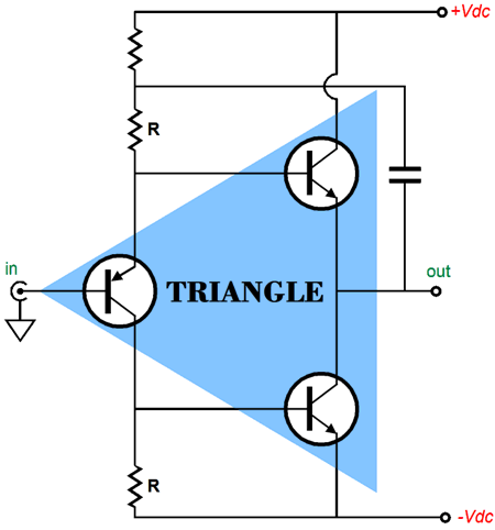
Bastode Anti-2gm Power Buffer The history behind the circuit's design is interesting. It was born from modifications to my triangle designs from post 232.
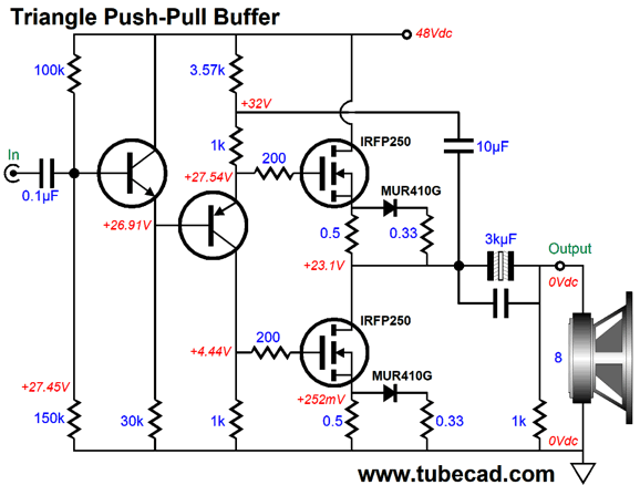
The triangle uses just three active devices to create a push-pull buffer. I believe the last time we saw a triangle buffer was back in post 386, which held the following circuit.
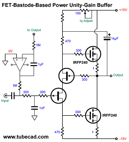
The above circuit is a power buffer capable of driving loudspeakers and is powered by a 48V switcher power supply; in addition, it is a constant-gm design. I very much like not using complementary devices, the P and N version, but the same output device top and bottom. The first thought I had was since the above design used two transistors at its input, why not configure them in a bastode topology and gets some gain and feedback going? Well, after I had created a fairly complex bastode-based power buffer in SPICE, which delivered fairly good performance, I decided to pull up one of my older but similar SPICE circuits to see how much of an improvement I had wrought. I hadn't, it turned out, as the simpler and older design outperformed the more complex and newer design. In post 418, I said: "Simple is easy. Effective is hard. Simple and effective is almost impossible. Welcome to existence." Well, it seems that I could amend this with, "Complex and effective is impossible." The following design moves us one step closer to the ideal. In fact, if we want to drive low-impedance headphones or just a high-efficiency tweeter, we could stop here with this pure class-A buffer.
The input is AC coupled through the coupling capacitor, as the input cannot be at ground potential. The OpAmp is configured as a DC servo-loop that keeps the output DC offset down to a few millivolts. The 100-ohm potentiometer at the top sets the idle current through the output stage, while the 1kµF capacitor equalizes the AC drive signals that the top and bottom MOSFETs see. Note the +/-15Vdc power-supply rail voltages, which allow us to use this bipolar power supply to directly power the DC servo's OpAmp. Also note the switch to FETs in the bastode circuit. Since we are going all out, these MOSFETs run in class-A. We could run an idle current of 500mA, which would result in a peak, class-A output current swing of 1A and a peak voltage swing of 8V, which into an 8-ohm load equals 4W. With a 100+dB horn tweeter, we would get plenty of sound. The same holds true for even the least efficient planar headphones. For most, however, a 30W power buffer would prove more appealing. How would we drive it to full output? All that is needed is a hot tube line stage amplifier capable of putting out 22Vpk of signal. An Aikido gain stage with a 12AY7/6072 input stage would do this easily.
Okay, to get 30W we will have to add more output devices.
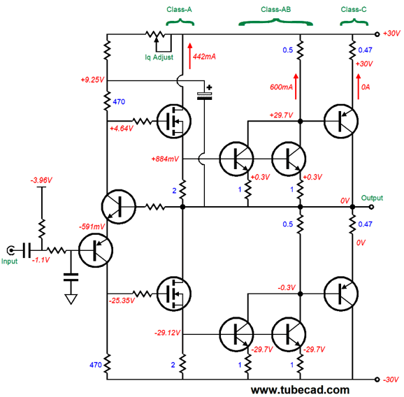
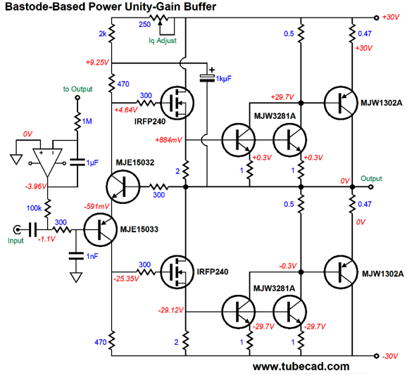
The FETs have been replaced by transistors. Why? High-voltage P-channel FETs are next to non-existent, whereas the PNP MJE350 can withstand 300V. The MJW3281A NPN transistors idle at 300mA each and they run in a rich class-AB. The MJW1302 PNP transistors run in class-C and do not conduct at all at idle. The result is that classes A + AB + C equals constant-transconductance.
How does the circuit above work? As the output swings positively, the bottom NPN transistors will eventually turn off, but just as they cease to conduct, the topmost PNP transistor begins to conduct, making up for the turned-off bottom transistors. Conversely, as the output swings negatively, the topmost NPN transistors will cut off, but at the same time the bottom PNP transistor will start to conduct, restoring constant gm. We can expect the MOSFETs to run the hottest at idle, followed by the four NPN transistors, while the PNP remain at room temperature. At full output, however, the MOSFETs will cool, while the NPN transistors get much hotter and the PNP transistors will warm up. The pure class-A window of operation extends a little over 16W into 8-ohm loudspeakers, which is crazy rich. Most solid-state output stages have a class-A window between 100mW to 1W, with most centering at 0.25W. Now, let's flesh-out the design.
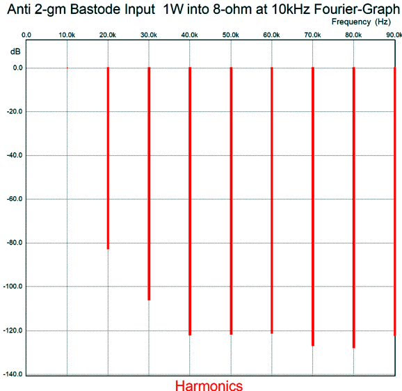
Here is the SPICE-generated Fourier graph for 4Vpk (1W) at 10kHz into an 8-ohm load with the final circuit.
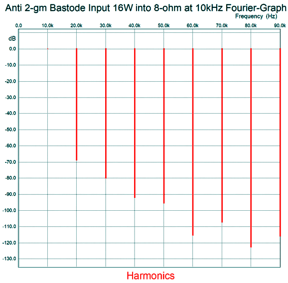
Four volts peak equals 1W into 8 ohms. Note the wonderfully single-ended cascade of harmonics, with a THD around 0.01%.. Now, let's look at 16W of output.
Still quite lovely and the THD is below 0.1%. We move on to full output, 30W.
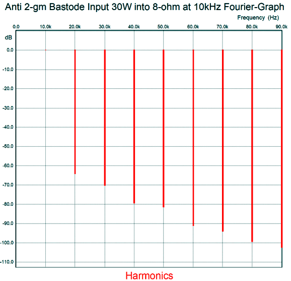
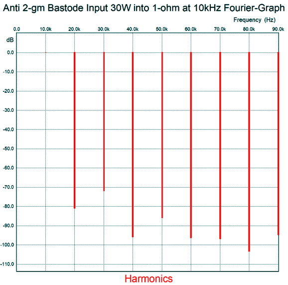
The single-ended pattern of harmonics persists, amazingly enough. The MOSFETs never turned off and the PNP transistors only turned on briefly. In SPICE simulations, the output impedance came in at below 8 milliohms, in spite of 1-ohm emitter resistors. Why does it work so well? Well one reason is that the top and bottom sets of MOSFET and transistors are matched. In other words, the same N-channel MOSFET is used above and below, as are the same NPN transistors. This means the usual arrangement of N- and P-channel MOSFETs or NPN and PNP transistors are not employed, so we do not have to pray that the different polarity devices perfectly complement each other, which never actually do in reality. Second, the buffer only consists of two stages, the bastode input stage and the output stage. Before signing off, I will mention that I have many SPICE tests to see how close an output stage comes to being constant-gm. One quick test is to use a 1-ohm load in place of an 8-ohm load and see what full power looks like. Here is the result of 30W at 10kHz (7.75Vpk) into 1 ohm.
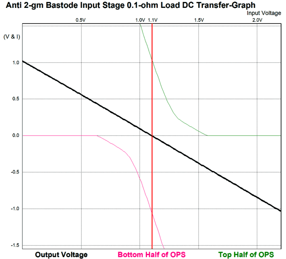
It looks far more push-pull in harmonic structure, which makes sense as the MOSFET no longer run in class-A, but still fine. In other words, this buffer is quite load invariant, which is a good feature, as most speakers are quite impedance variant. Here is a DC transfer graph, which shows how linear the buffer is with a 0.1-ohm load resistance.
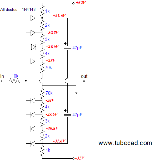
Ruler straight. Okay, what is the catch? Well, first of all, eight big output devices are used to produce only 30W, whereas a more conventional amplifier could get 200W out of eight output devices. Second, its huge class-A window of operation results in a lot of heat, a little over 60W at idle, whereas most solid-state 30W amplifiers are cool to the touch at idle. Third, the +/-30Vdc power-supply rail voltages could deliver closer to 45W with a more conventional design. Fourth, and the only problem that actually bothers me, the buffer does not clip as smoothly as I would like. One workaround to the last problem is to use my soft-clipping circuit from post 66.
I am entirely convinced that one of the best attributes of tube amplifiers is their relatively soft clipping when compared to most solid-state efforts. All amplifiers clip, but some do so more egregiously than others.
//JRB
Schematic Typo
If you enjoyed reading this post from me, then you might consider becoming one of my patrons at Patreon.com
User Guides for GlassWare Software
For those of you who still have old computers running Windows XP (32-bit) or any other Windows 32-bit OS, I have setup the download availability of my old old standards: Tube CAD, SE Amp CAD, and Audio Gadgets. The downloads are at the GlassWare-Yahoo store and the price is only $9.95 for each program. http://glass-ware.stores.yahoo.net/adsoffromgla.html So many have asked that I had to do it. WARNING: THESE THREE PROGRAMS WILL NOT RUN UNDER VISTA 64-Bit or WINDOWS 7 & 8 or any other 64-bit OS. I do plan on remaking all of these programs into 64-bit versions, but it will be a huge ordeal, as programming requires vast chunks of noise-free time, something very rare with children running about. Ideally, I would love to come out with versions that run on iPads and Android-OS tablets. //JRB |
John Gives
Special Thanks to the Special 68
I am truly stunned and appreciative of their support. In addition I want to thank
All of your support makes a big difference. I would love to arrive at the point where creating my posts was my top priority of the day, not something that I have to steal time from other obligations to do. The more support I get, the higher up these posts move up in deserving attention. Only those who have produced a technical white paper or written an article on electronics know just how much time and effort is required to produce one of my posts, as novel circuits must be created, SPICE simulations must be run, schematics must be drawn, and thousands of words must be written. If you have been reading my posts, you know that my lifetime goal is reaching post number one thousand. I have 579 more to go. My second goal is to gather 1,000 patrons. I have 932 patrons to go. Help me get there.
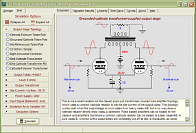
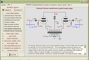
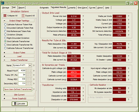
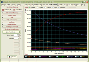
Support the Tube CAD Journal & get an extremely powerful push-pull tube-amplifier simulator for TCJ Push-Pull Calculator
TCJ PPC Version 2 Improvements Rebuilt simulation engine *User definable
Download or CD ROM For more information, please visit our Web site : To purchase, please visit our Yahoo Store: |
|||
| www.tubecad.com Copyright © 1999-2018 GlassWare All Rights Reserved |

