| John Broskie's Guide to Tube Circuit Analysis & Design |
17 July 2020 Post Number 508
Push-pull Auto-Cathode-Bias
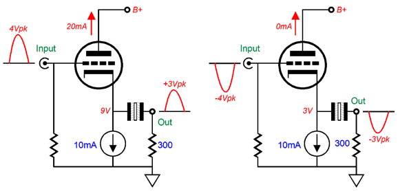
This is a cathode follower with constant-current source loading. The cathode follower must do all the work, as the constant-current source presents a constant downward tug. As a result, the maximum theoretical efficiency we can obtain is 25%, which with real triodes and pentodes is wildly optimistic, with actual efficiencies of 5% to 10% being impressive. (Resistive loading is even less efficient, coming in at a theoretical efficiency a tad better than 8%.) Still, we don't use tubes to save energy. Here is an example of the maximum peak current swings possible with a constant-current source loaded cathode follower driving a 300-ohm load impedance.
A 4Vpk input signal prompts the cathode to swing positive by 3Vpk. The triode's current conduction peaks at twice its idle value. The 300-ohm load sees a peak current flow of 10mA, and the constant-current source continues to draw 10mA. When the input signal swing negative to -4Vpk, the cathode voltage falls by -3Vpk. This time, the triode ceases to conduct and the constant-current source pulls the output down by -3Vpk. The 300-ohm load dissipates 15mW of power. If the cathode-top voltage is 100V, the triode's plate dissipates 1W of heat at idle, resulting in an efficiency of only 1.5%.
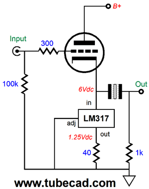
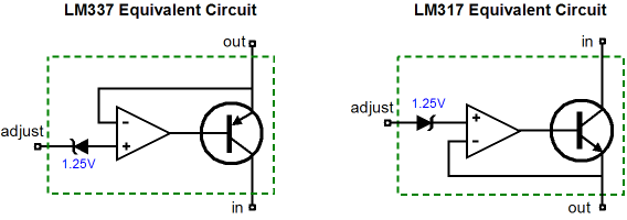
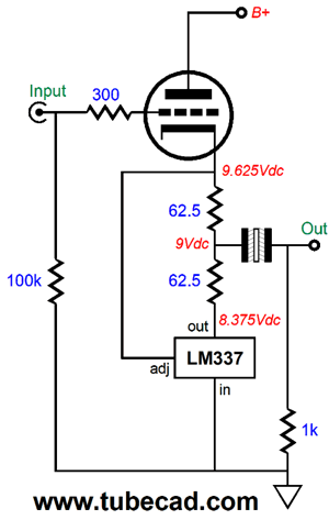
Few know that we can use in the place of the LM317 its equivalent negative version, the LM33. Why bother? One answer is that the LM337's tab can be grounded to the chassis; and, if nothing else, the tab will be at ground potential, so no shock hazard exists. I mentioned this starting back in 2004, but few listened.
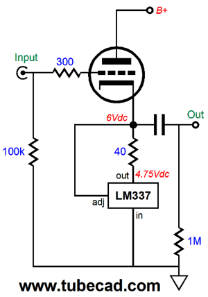
An additional advantage delivered by the LM337 is the creation of a class-A push-pull output, as using two cathode resistors and an LM337 not only yields constant-current source auto-bias, it creates a class-A push-pull output stage. Think of it as an upside-down hybrid SRPP.
In contrast to the single-ended version loaded by the constant-current source, twice the idle current is potentially available as the peak output current swing. Now, if we double the peak current swing, we also quadruple the power output, as power = I²R/2. For example, 10mA peak swings into a 300-ohm load equals 15mW of power; but 20mA current swings equals 60mW.
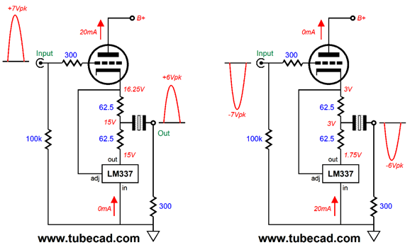
The operation is similar to the single-ended version, but bigger. A 7Vpk positive input signal forces the cathode voltage to swing positively by 6Vpk. Much like the single-ended version, the triode's current conduction peaks at twice its idle value, but this time the 300-ohm load sees a peak current flow of 20mA, not 10mA, while the LM337 stops conducting altogether. When the input signal swings negatively by -7V, the triode stops conducting and the LM337 pulls the output down by -6Vpk. The result is the fourfold increase in power output, going from 15mW to 60mW, which in turn means that the resulting efficiency is 6%, not 1.5%. Note that the triode works just as hard as it did before with the LM317, yet the power output went up by fourfold. The LM317 and LM337 cost about the same and adding one extra cathode resistor is not that expensive In short, we gain a fourfold increase in output power at minimal cost. I can imagine many fearing that the LM337 was too lowly a solid-state device for serious audio gear. Okay, why not make our own LM337 replacement out of discrete devices?
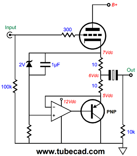
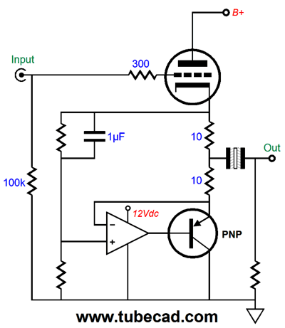
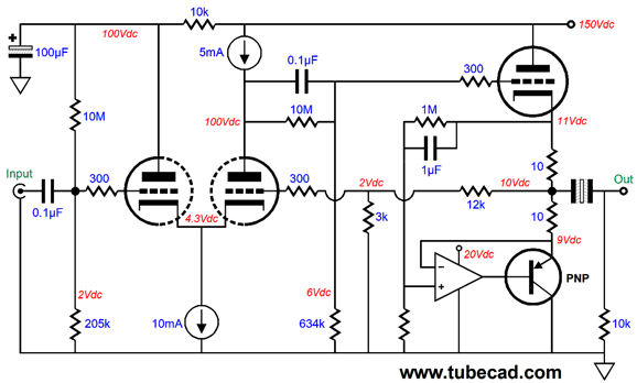
The OpAmp drives the PNP transistor and delivers unity gain. The 2V voltage reference sets the voltage drop across the two 10-ohm cathode resistors in series. The see how the push-pull operation works, imagine the output shorted to ground and the output coupling capacitor and 10k resistor replaced by a 6V battery.
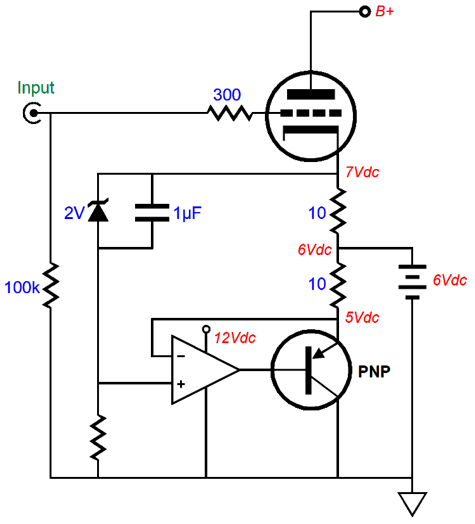
If the cathode voltage rises, the OpAmp will force the PNP transistor's emitter voltage to follow. However, the nexus between the two resistor remains fixed at 6Vdc. If the cathode rises by 1V, the triode's current conduction will have doubled, while the PNP transistor's conduction will have fallen to zero. If the cathode voltage falls by 1V, the triode will cease to conduct, while the PNP transistor's conduction doubles. In other words, the battery would source and sink 200mA, which is twice the idle current flow. Okay, now imagine a 16-ohm load. When the triode conducts at twice its idle current of 100mA, the peak 200mA will develop 3.2Vpk across the 16-ohm load impedance and the PNP transistor will conduct zero current. The cathode voltage will equal 2Vpk added to 3.2Vpk, making for a total of 5.2Vpk. The voltage drop across the bottom 1-ohm cathode resistor will equal 0V. When the output signal swings to its negative peak of -3.2V, the triode will cease conducting and the PNP transistor will conduct 200mA peak. At all times, the voltage drop across both cathode resistors will equal 2V. In a nutshell, this is perfect class-A push-pull operation. We do not have to use a voltage reference, as we can use a resistor instead.
Assume that both resistors in the two-resistor voltage divider that starts at the cathode and terminates into ground share the same value, say 100k. In DC terms, the result is that the two 10-ohm cathode resistors effectively double in value, acting as if a single 40-ohm cathode resistor were used to cathode-bias the triode. In AC terms, the cathode is loaded by a constant-current source and whatever external load impedance is driven times two. Because this is a class-A push-pull output stage, the external load impedance appears twice as large to the triode than it actually is. In a class-B output stage, each output device sees the load as it actually is. In a class-AB output stage, in the small class-A portion of the output current swing, the load appears to be twice its actual value. Once the output stage leaves its small class-A window of operation, the load falls to its nominal value and the output impedance doubles. This is gm doubling. Let's look at buffed up version, wherein the triode gets some super-triode enhancement.
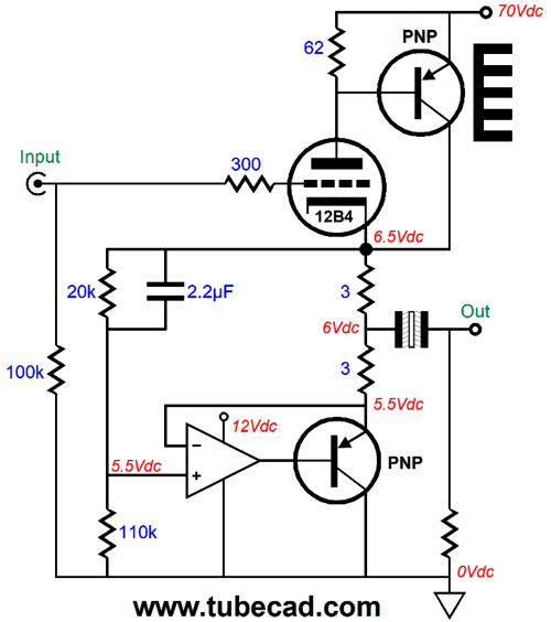
The idle current is a heavy 166mA. The PNP transistor will dissipate about 10W. Due to the high idle current, we can get well over 1W into a 32-ohm load. By the way , we can also use a pentode, although the pentode (a KT88) is in the triode-connected configuration.
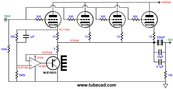
Note the PNP-NPN compound configuration. In addition, we can place several triodes in parallel.
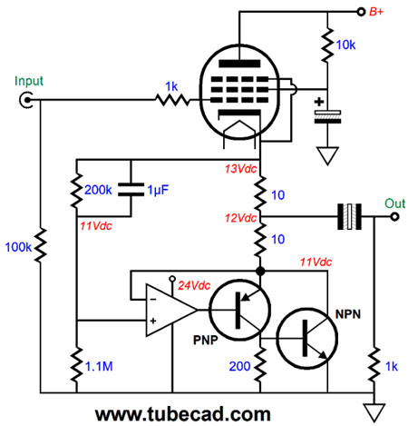
Note that each triode gets a 12-ohm cathode resistor, while the MJE15033 gets a 3-ohm emitter resistor. We can make a complete amplifier, in the following example, a headphone amplifier.
Note the DC and AC negative feedback, as the 3k feedback resistor terminates into ground directly, not into a capacitor.
Error-Correcting MOSFET Output Stages The idea is simple: correct problems at the source, then apply the global feedback loop. If we stop and think it over, we see that the compound output stage belongs to this second group of nested-feedback amplifiers, as the compound circuit's enslaved output devices and master driving transistors form nested local negative feedback loops in themselves.
In fact, Daniel Meyer's SWTC Tiger 01 amplifier used a compound output stage and a nested negative feedback loop, one feedback loop within another within another.
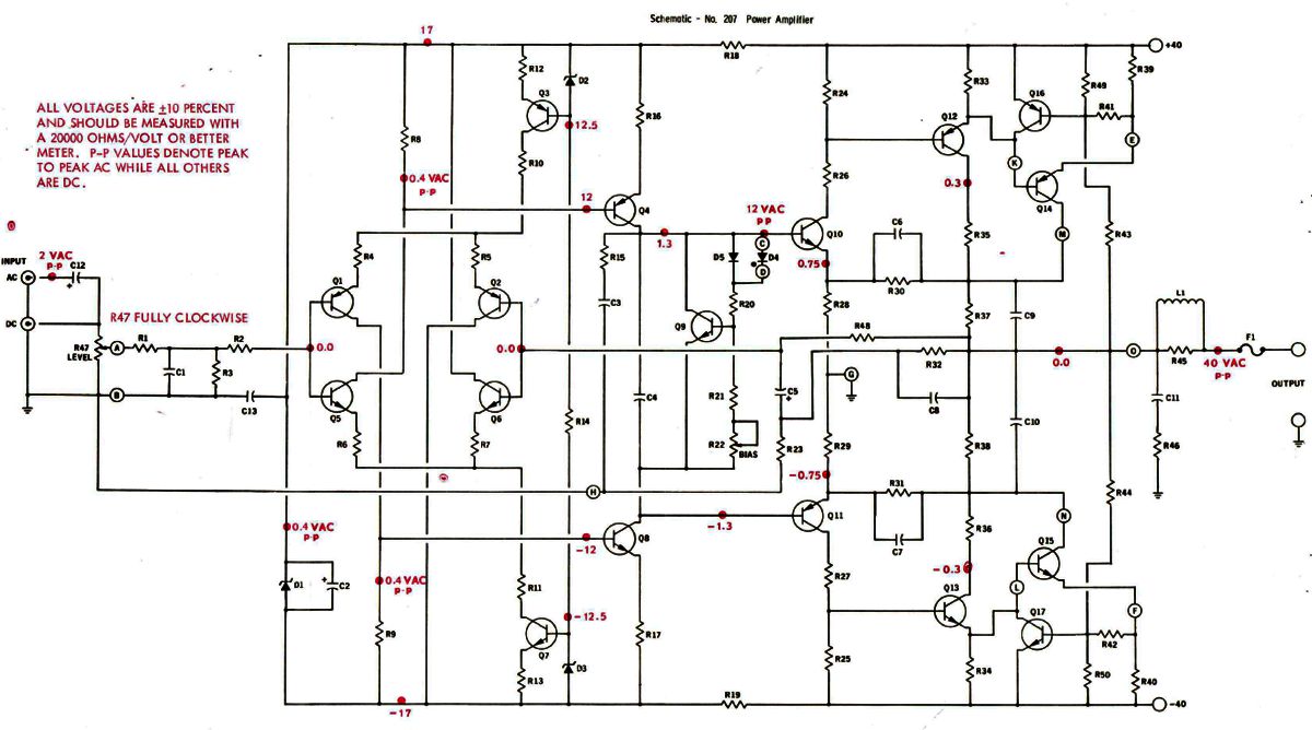
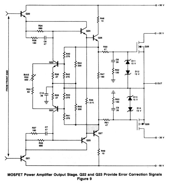
Note that 12Vac becomes 40Vac at the output, which implies a gain of 3.3 for the output stage. Also note that the output stage runs off of +/-40Vdc, while the input and VAS stages run off the lower +/-17Vdc power-supply rails, which see a zener shunt voltage regulation. (Well, almost. If two zeners had been used and if both terminated into ground, we would have something closer to true shunt regulation.) If Q16 and Q17 are making you scratch your head, they are there to limit the maximum dissipation from Q14 and Q15, the output transistors. Also worth noting is the fully complementary and symmetrical layout between top and bottom. As I understand it, John Curl came up with an earlier version in the late 1960s, but kept it a trade secret.
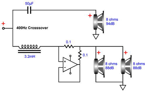
Okay, so much for ancient history. What sent me down this path was my reviewing some of my unity-gain power buffer designs, as I was looking for some design that could be converted into an impedance-multiplier circuit (IMC) to be placed within a loudspeaker enclosure and run off an external 48Vdc switcher power supply. The idea was that a flea-power tube amplifier could drive a high-efficiency fullrange driver (94dB SPL), while the IMC drove a pair of two low-efficiency (88dB SPL) woofers, resulting in an impedance of 4 ohms, but which the IMC reflects as 8 ohms to the tube amplifier.
If we move the crossover's inductor to the other side of the IMC, between the IMC and the two woofers, we can use an inductor with half the inductance. The down side, however, would be that the IMC would have to handle the entire audio bandwidth. Here is the unity-gain power buffer design that I thought looked promising.
This is a class-A, push-pull power buffer that could deliver 16W into 8-ohm loads. In addition, it auto-biases the output devices. I kept searching through my SPICE circuits and I found an even simpler power buffer.
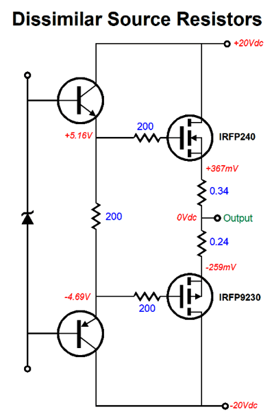
This unity-gain power buffer receives its input at the input transistors emitters and auto-biases for class-A push-pull operation. The input impedance is relatively low, about 8k, but that would not be a problem if driven by a power amplifier, even a flea-power tube amplifier. By the way, the reason that the top MOSFET, the N-MOSFET, gets two source resistors is that the N-channel MOSFET exhibits higher transconductance than the bottom MOSFET and the extra 0.1 ohms of source resistance evens things up.
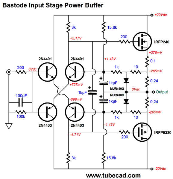
As I looked the circuit over, I wondered if it could not be used as a nested feedback output stage inside a larger power amplifier. This is when all the previous nested-feedback designs came to mind, especially Bob Cordell's, as he had used the relatively huge MOSFET turn-on voltages to create a small voltage window within which to operate an elaborate negative feedback system.
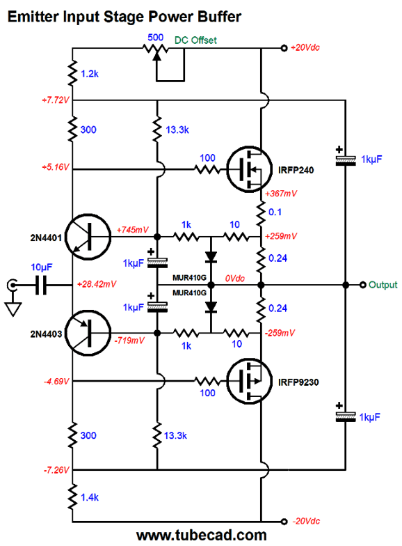
Shown above is Cordell's design. Yes, it's complicated, but not impossible to unravel. It's interesting, but I wanted to keep as much of my original design as possible. The problem I faced was that I needed to find a way to feed the clean input signal into the input transistor emitters and retain the class-A auto-bias feature. Then it came to me.
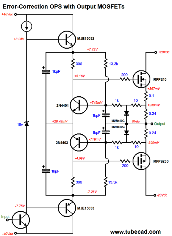
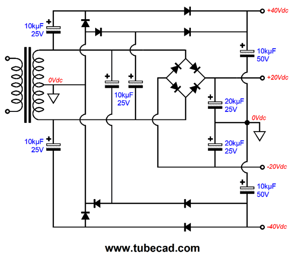
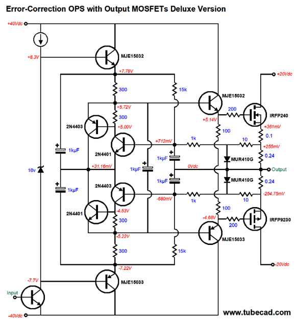
The two 1kµF capacitors attach to the joined emitters and relay the clean signal from the MJE15032 and MJE15033 driver transistors emitters. (By the way, we can bypass these two capacitors with two 1k resistors.) The 2N4401 and 2N4403 transistors evaluate the output signal to the input signal at their emitters. If the output fails to match the input signal, these transistors adjust their collector voltage to bring the two output MOSFETs inline. The two MUR410G diodes are there to clip the error-correction transistors DC signal at twice the idle value. With an idle current of 1.1A, we can expect a peak output voltage swing of 17.6V into 8-ohm load, which implies 19W of output power. This assumes that the +/-20V power-supply rails do not collapse. If we limit ourselves to 16Vpk, we get 16W of output power. The biggest departure from typical solid-state output stages just might be the two sets of bipolar power supply voltages, +/-20Vdc and +/-40Vdc. The VAS (voltage amplification stage) and driver stage must use a higher power-supply rail voltage to overcome both the voltage overhead required for the error-correction circuit and to deliver the needed drive voltages for the output MOSFETs. Note that if we had used just a +/-20Vdc bipolar power supply, we could only get a fraction of the possible output voltage swings. Is our having to use two power-supply-rail voltages a deal breaker? Not at all, as we can easily build a multi-rail, full-wave bridge bipolar power supply.
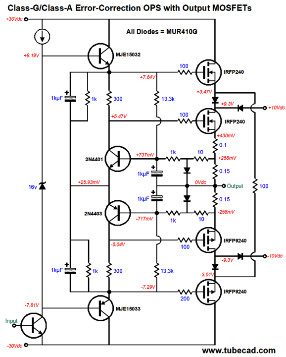
In fact, our having two power-supply rail voltages allow us to get extra clever, as we could set up a class-G output stage.
Note the +/-10V and +/-30Vdc bipolar power supply voltages. In addition, the idle current is set to a hot 1.7A. Why so high? Class-A operation. This output stage weds class-G to class-A push-pull output. Moreover, the class-a operation extends to the class-G MOSFETs, they never turn off. At idle, they continue to conduct about 80mA through the 100-ohm resistor that bridges both sources. Without this resistor, which 100% of existing class-G amplifiers do not include, the class-G MOSFETs would be turned off at idle and then must be summoned to awake and conduct when needed, which creates all sorts of headaches, such as inductive voltage spikes and switching distortions. In contrast, never letting them turn off makes for smooth sailing. Think of it as class-A running of the class-G MOSFETs. Okay, what further hotrod modifications are possible? We could give the output MOSFETs an emitter-follower driver stage, and we could increase the error-correction transistor's gain by compounding them.
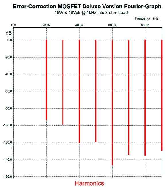
The additional 1kµF capacitor tightens the unity of the OPS as a single circuit. How well does topology work? Here is the SPICE-generated Fourier graph for full output (16W) at 1kHz into an 8-ohm load.
Remember this is just an output stage. A complete amplifier would include an input stage and voltage amplification stage (VAS) and global negative feedback loop, which would further lower the distortion and output impedance and increase the PSRR. By the way, we could use output transistors, but we will have to forgo the compounding of the error-correction transistors.
Note that the error-correction transistor's collector resistors are no longer 300 ohms, but 750 ohms, which results in greater gain and, thus, more error-correction. Here is its Fourier graph of full output.
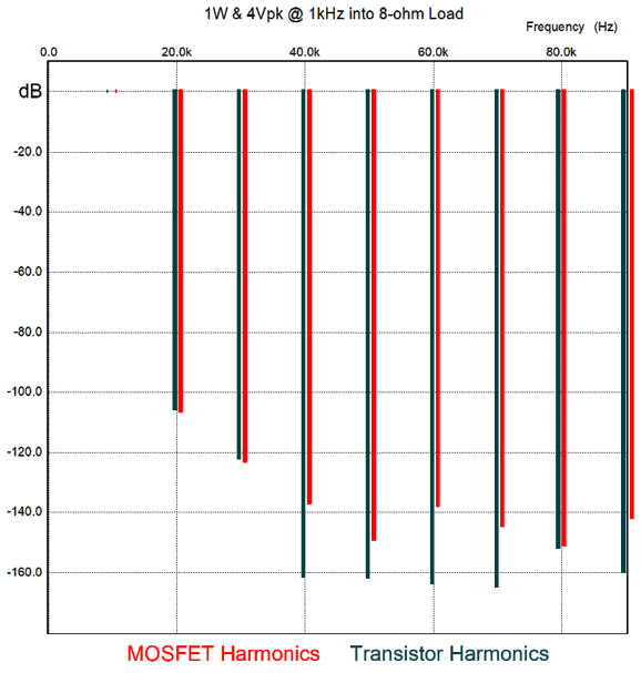
I prefer the MOSFET version, but at 1W of output the transistor version produced less distortion.
The only MOSFET harmonic that is lower is the 2nd.
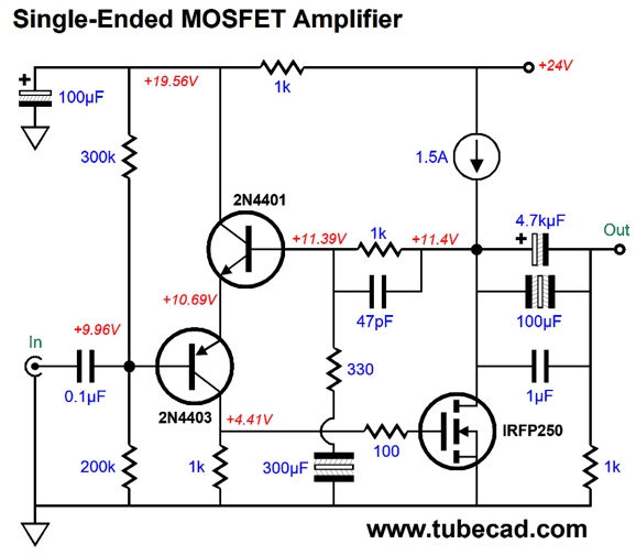
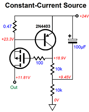
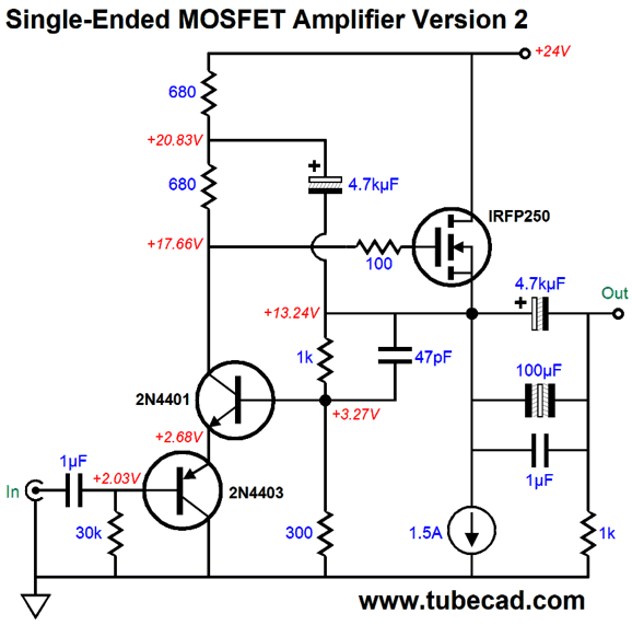
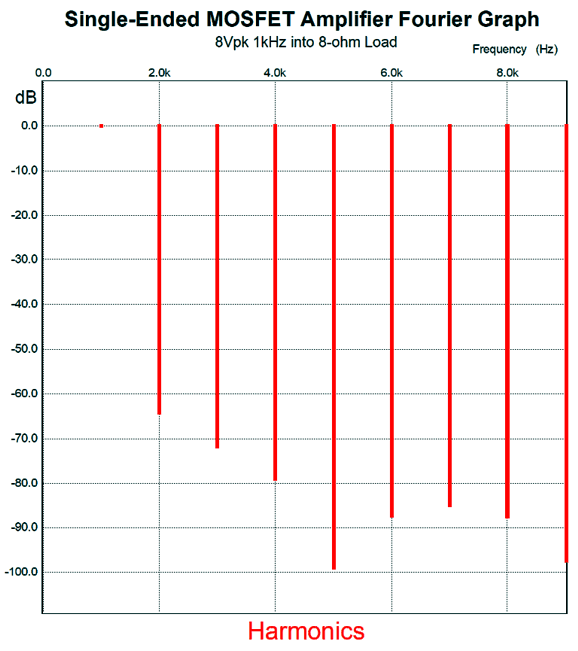
Single-Ended MOSFET Amplifier The following design is very Zen-like, as a single power MOSFET does all the hard work.
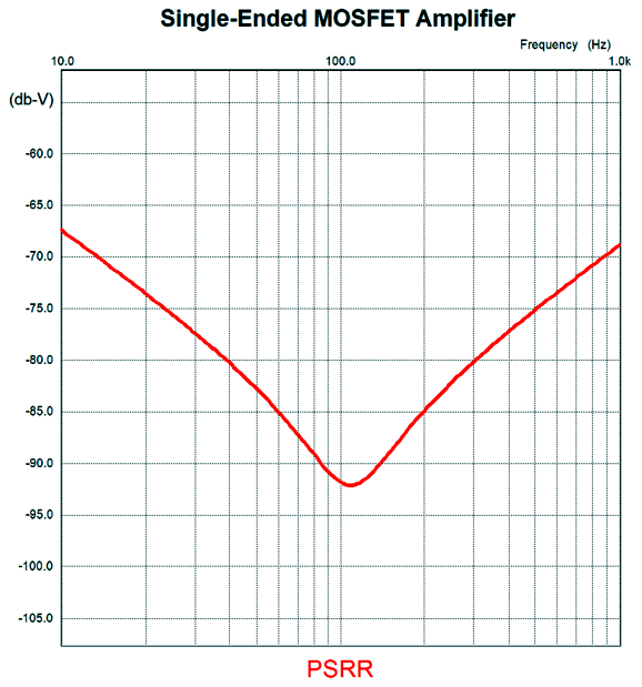
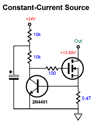
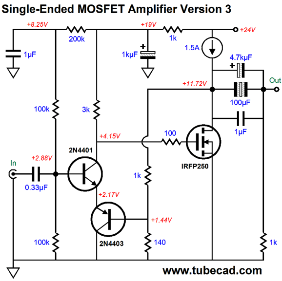
A bastode input stage functions as a differential amplifier that compares the output signal to the input signal and adjusts the MOSFET's current conduction to force the output signal to conform. The 1k and 330-ohm resistors form the negative feedback loop and set a gain of roughly 4 (+12dB), so an input signal of 2Vpk is needed to drive the amplifier to full output, i.e. 8Vpk and 4W into an 8-ohm loudspeaker. The output coupling capacitors are arrayed in parallel to provide the best sound. The -3dB low-frequency cutoff occurs at 5Hz. For bandwidth down to only 20Hz we only need a 1kµF coupling capacitor. The formula is simple enough: Capacitor = 159155/Frequency/Resistance Where the result is in µF. If we wanted to limit the bandwidth down to 100Hz, we would use a 200µF capacitor, which is small enough to allow us to use two 100µF film capacitors in parallel. The 330-ohm negative feedback loop resistor terminates into a 300µF non-polarized electrolytic capacitor, which could be (and should be) bypassed by a small film capacitor. The constant-current source can be made from several LM337 three-pin, adjustable voltage regulators in parallel, each configured as a constant-current source. Alternatively, we could use a power P-channel MOSFET. The PNP transistor controls the P-MOSFET's current conduction by monitoring the voltage drop across the 0.47-ohm source resistor. The 100µF capacitor improves the constant-current source's PSRR. An alternative topology uses the N-MOSFET as a source follower. The bastode input stage must develop the large drive signal needed to drive the output MOSFET to full power, once again, 4W and 8Vpk into 8 ohms. The negative feedback loop terminates directly into ground, but the 4.7kµF capacitor is still needed to bootstrap the bastode's collector resistor, which allows the collector voltage to swing above the 24V power-supply rail voltage. In addition, this capacitor shields the resistor from the power-supply noise. No doubt, the 4.7kµF value seems crazy high. It isn't. We need such a large value to center the PSRR deepest dip at 120Hz. The constant-current source can be the inversion of the previous example, using an N-MOSFET instead of a P-MOSFET. In SPICE simulations, the constant-current source drew 1.46A of current, which means that the output stage will dissipate 35W per channel. Very toasty, indeed. In other words, a large heatsink will be needed. No one ever claimed that class-A was cheap. How big a heatsink is needed depends on how hot you are willing to let the heatsink become. For example, say that we set a limit of 60C (140F) and that the room temperature is 25C (77F), then we subtract 25C from 60C and 35C, which divided by 35W equals a thermal resistance of 1C/W. This calculation assumes a monoblock power amplifier. For a stereo amplifier, the thermal resistance would need to be halved to 0.5C/W. Although I used an IRFP250 in my SPICE simulations, I would actually use an IRFP260MPbF, as it offers a 300W rating. Speaking of SPICE simulations, the distortion characteristics are interesting.
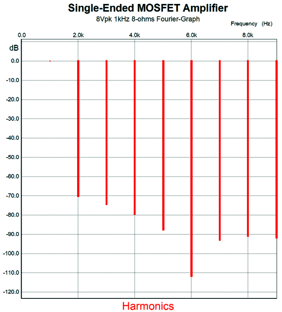
Note the extra suppression of the 5th harmonic and the single-ended nature of the declining harmonics. The first version offered a different set of harmonics.
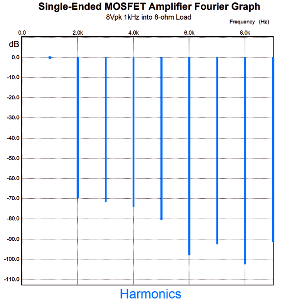
Note that this time, its the 6th harmonic that gets the extra attenuation. Which is better? Although the second design's THD is slightly higher, I bet the first would sound better, as most of its distortion is 2nd harmonic and its lower 5th, 7th, and 9th harmonics seal the deal. Okay, I thought I was done, but no. I just thought of a third variation on this theme. The two previous version offered a gain 4 (+12dB); this version delivers twice the gain, 8 (+24dB). Is that important? It is if you want full output with 1Vpk of input signal.
Notice how we were able to squeeze the bastode transistors within the MOSFET's gate voltage of 4.15V. My big fear was that since the gain was doubled, the THD would dramatically increase. It didn't.
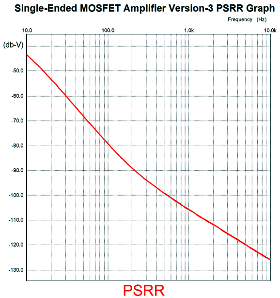
The THD is below 0.1% at full output. The PSRR is excellent.
Focus on 100Hz and 120Hz, as those are the ripple frequencies, depending where you live. No doubt that some are wondering if a larger scale version could not be made, say with a 48Vdc switcher power supply, so much more power could be had. It could, but it would require a 3A constant-current source and four output MOSFETs. Such an amplifier could swing 20Vpk, which would equal 25W of single-ended class-A power. Mercy. The efficiency would come in at 17.4% and one channel would dissipate 144W at idle.
Music Recommendation: Alexis Ffrench's Evolution The recording is excellent. I listened to the Amazon Music high-res version, which offered 24-bit at 96kHz. If I had to find something to complain about it would be that some of his compositions stray dang close to schmaltzy, but then you must remember that my taste leans toward austere and angular. In fact, I can easily imagine my playing his album at a family get-together and not be pummeled by requests for a different album. At Amazon Music, we find 32 albums and solo tracks by Ffrench. If only one tenth of his works survive and become standard concert-hall repertoire, he will leave a big mark on classical music.
//JRB
User Guides for GlassWare Software
For those of you who still have old computers running Windows XP (32-bit) or any other Windows 32-bit OS, I have setup the download availability of my old old standards: Tube CAD, SE Amp CAD, and Audio Gadgets. The downloads are at the GlassWare-Yahoo store and the price is only $9.95 for each program. http://glass-ware.stores.yahoo.net/adsoffromgla.html So many have asked that I had to do it. WARNING: THESE THREE PROGRAMS WILL NOT RUN UNDER VISTA 64-Bit or WINDOWS 7 & 8 or any other 64-bit OS. I do plan on remaking all of these programs into 64-bit versions, but it will be a huge ordeal, as programming requires vast chunks of noise-free time, something very rare with children running about. Ideally, I would love to come out with versions that run on iPads and Android-OS tablets.
|
I know that some readers wish to avoid Patreon, so here is a PayPal button instead. Thanks. John Broskie
John Gives
Special Thanks to the Special 81 To all my patrons, all 81 of them, thank you all again. I want to especially thank
I am truly stunned and appreciative of their support. In addition I want to thank the following patrons:
All of your support makes a big difference. I would love to arrive at the point where creating my posts was my top priority of the day, not something that I have to steal time from other obligations to do. The more support I get, the higher up these posts move up in deserving attention.
If you have been reading my posts, you know that my lifetime goal is reaching post number one thousand. I have 492 more to go. My second goal was to gather 1,000 patrons. Well, that no longer seems possible to me, so I will shoot for a mighty 100 instead. Thus, I have 19 patrons to go. Help me get there.
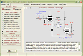
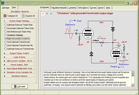
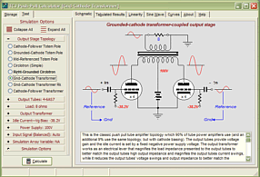
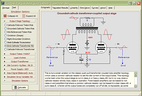
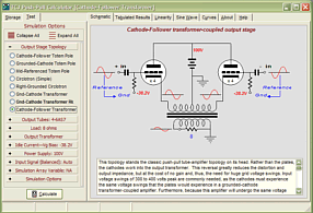
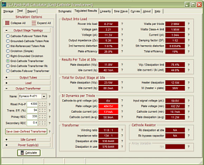
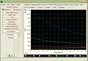
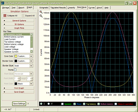
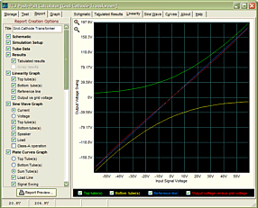
Support the Tube CAD Journal & get an extremely powerful push-pull tube-amplifier simulator for TCJ Push-Pull Calculator
TCJ PPC Version 2 Improvements Rebuilt simulation engine *User definable
Download or CD ROM For more information, please visit our Web site : To purchase, please visit our Yahoo Store: |
|||


| www.tubecad.com Copyright © 1999-2020 GlassWare All Rights Reserved |