|
For example, the popular MJ15003 NPN power transistor lists a range of 25 to 150 for its hFE. Thus, making a useable transistor-based buffer with just three transistors is difficult, given the actual potentially low hFE of most transistors; with less than three transistors, it is near impossible. |
|
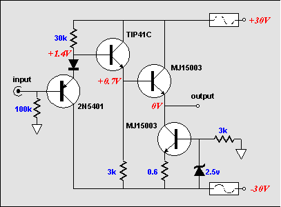
Reader Tony's 3-stage, single-ended, Class-A buffer |
||
|
Hand selecting high-hFE transistors might give an adequate current gain, but a safer bet would be to add a fourth transistor. An added transistor would not only increase the final current gain, but would also eliminate the need for the first stage's diode. Each transistor has about a .7 volt drop from base to emitter. Thus, cascading PNP to NPN to PNP to NPN transistors should keep the output's DC offset inline with the input. Now, adding more stages to an amplifier is usually fraught with danger, as each stage introduces some phase lag, which in an amplifier that uses a global feedback loop potentially spells oscillation. In an amplifier that forgoes global feedback in favor of local feedback, the phase shift is of no real concern, but at the cost of dropping frequency response at the extreme high frequencies and higher output impedance. |
|
One solution is to decrease the resistors' value, so as to allow for the increased current demand of the following stage. This would certainly help. However, it would also greatly increase the required current gain for the amplifier as whole and it would also greatly increase the dissipation of the transistors. Another solution would be to use a separate, higher voltage power supply for the input and driver stages. This would allow lower idle currents to be used and would increase the linearity of the emitter followers. However, it would also greatly increase the voltage breakdown requirements for the transistors. |
|
|
||
Pg.
10