|
More ð |
|
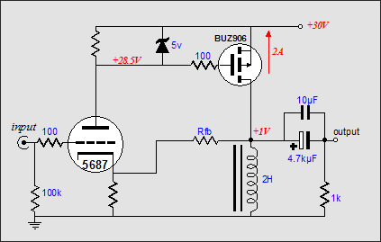
The amplifier to the right is single ended and uses a choke to load the P-channel MOSFET. The DCR of the choke against the idle current defines the DC offset. If the DCR is low enough, the coupling capacitors could be jettisoned. If the amplifier were to be used in a bi-ampped system, with the it powering the higher frequencies, then the crossover capacitor could do double duty as the output coupling capacitor. |
|
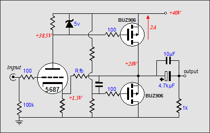
This next amplifier uses the same basic idea, but replaces the inductor with MOSFET based constant-current source. The B+ had to be raised to allow more voltage swing, as the constant-current source cannot swing below ground the way the inductor can. (“Constant-current source,” like so many terms in electronics, is a misnomer, as a true source would be able to provide its own voltage and current. A better name for this type of circuit is “constant-current regulator,” as it only regulates the amount of current flow. A 1Meg resistor placed across a true 1A constant-current source would see 1,000,000 volts develop across its leads.) |
|
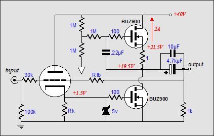
The amplifier to the right uses N-channel MOSFETs (which I prefer) and will more reliably self-center. (Note that all three of these amplifiers will exhibit a good deal of second-harmonic-distortion, as the triode will turn on more readily than it will turn off and the same holds true for the MOSFET, thus the two device's non-linearity are going in the same direction, which means that curvature will compound, not subtract. Still, there is a negative feedback loop to lower the output impedance and distortion. Furthermore, all three of these simple amplifiers require strict class-A operation, which means heat and massive power transformers.) |
|
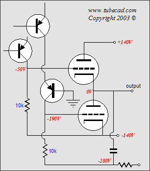
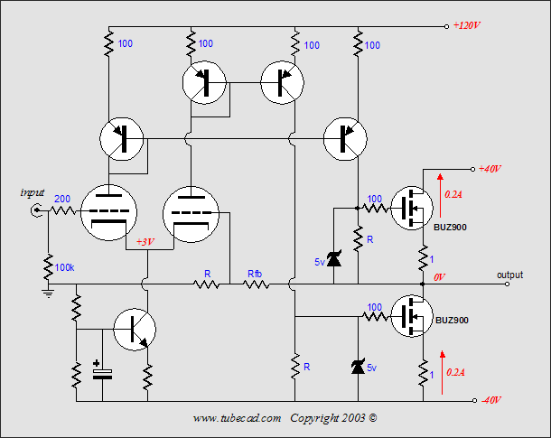
In contrast, the circuit above can be run in class-A, B, AB. Two current mirrors relay the tube-based differential amplifier’s balanced current swings to two resistors. One resistor terminates into the output and the second terminates into the negative power supply rail. Thus each output MOSFET sees the same magnitude of drive voltage, but in opposing phase. With the feedback loop closed, the triodes are in charge. In the absence of a negative feedback loop, this amplifier would have a near infinite output impedance and excessive gain. The current regulator that loads the triodes’ cathodes also sets the idle current of the output stage. As it stands, this amplifier close to being truly functional. What’s missing is output stage Zorbel-type networks and a means by which the DC offset could be adjusted. The obvious solution, a potentiometer that spans both cathodes is a poor choice, as potentiometers can break contact at times or become scratchy. A better idea is to use a pair of parallel and series resistors to reduce the potentiometer’s possible malfunctioning, as shown above. Of course a DC servo loop could replace the potentiometer altogether. As for output devices, other MOSFETS or, even, NPN transistors could readily be used. In fact, vacuum tubes could be used with the addition of coupling capacitors and negative bias power supplies… or something like what you see to the right. Here the two current mirrors connect directly to the output tubes’ grids. Both triodes function as cathode followers, which means that the global feedback ratio would be greatly reduced. The extra PNP whose base is grounded creates a cascode-like structure that prevents the PNP transistors from seeing too much voltage (300 volts is pretty much the voltage limit for PNP transistors). //JRB |