| John Broskie's Guide to Tube Circuit Analysis & Design |
25 February 2024 Post Number 597
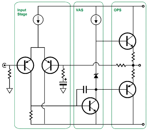
Acoustat Trans-Nova Power Amplifier In the strongest possible contrast, the Trans-Nova-amplifier topology departs from all the solid-state amplifier conventions. For example, three feedback loops are used; its VAS is a push-pull design, not a single-ended one; its output stage (inverting) delivers signal gain and requires a floating bipolar power supply and holds no current-limiting circuitry; none of its output power MOSFETs (six of them per channel) get a source resistor; instead, all its output-MOSFET sources terminate directly to ground; and no bipolar transistors are used, only MOSFETs.
Before we move on to its schematic, let's give the standard Lin topology, the 1950's solid-state amplifier design by Mr. Hung Chang Lin of RCA, a quick review. (Several times, I have been told that the Brits created the Lin topology, with either UK companies, Linn or Naim, or Mr. Douglas Self getting the credit. The Linn-Lin name confusion I can understand, but I doubt that Linn or Naim or Doug existed at all in the 1950s.)
From my post 574:
This is the near universal solid-state amplifier topology. Of course, we can get extra fancy, adding current mirrors and cascoded transistors and output current-limiting circuitry or by making the circuit fully complementary symmetrical, but the core Lin topology remains constant. The only features the Transnova shares the Lin topology is the differential input stage and one of its three feedback loops. By the way, "Transnova" stands for TRANSconductance NOdal Voltage Amplifier. If we accept (the American art historian) Bernard Berenson's definition of genius, "as the capacity for productive reaction against one's training," then surely James C. Strickland, the inventor of the Trans-Nova topology, was a genius.
Strickland labels the three feedback loops A, B, and C. A stands for anisotropic; B, Black classic negative feedback, after Harold Stephen Black, whose 1927 invention of negative feedback revolutionized electronics; and C, complementary, which means positive feedback. Here is the big-picture overview of the amplifier:
The first stage is non-inverting, but the following two stages do invert, which cancel, so the output is non-inverting. Thus, the B negative-feedback loop works the same way it would in a more conventional amplifier. Complementary feedback is simply positive feedback, which increases the first stage and second stage gain. The anisotropic feedback loop transforms the output stage into a current-to-voltage converter circuit; it functions as negative feedback.
By the way, "isotropic" means identical in all directions; invariant with respect to direction. "Anisotropic" means that direction matters. For example, a plank of wood presents different attributes depending on the direction, being stronger or more pliant in one direction, due to its wood grain; thus, it is anisotropic. If we grind up the wood and make paper from it, however, we get the resulting isotropic paper, as the wood grain no longer exists. In other words, we really only need two adjectives to describe the three feedback loops: negative and positive. Here is the simplified version of the Trans-Nova Twin-200 amplifier:
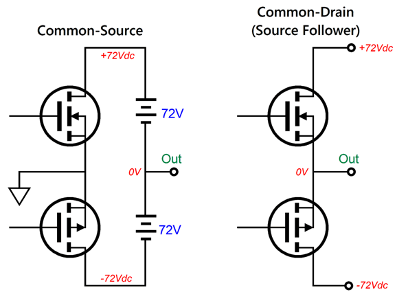
Note relatively high output stage rail voltages ( ±72V) and the relatively low amplifier frontend rail voltages ( ±23Vdc). Each channel's output stage must get its own floating bipolar power supply, but both channels can share the same ±23Vdc rail voltages. This improves upon the circlotron, as the circlotron requires two floating power supplies per channel. By the way, floating means no direct connection to ground. I used the battery symbol to override the mind's habit of knowing only grounded power supplies. Here is what an actual floating power supply might look like.
Note relatively high output stage rail voltages ( ±72V) and the relatively low amplifier frontend rail voltages ( ±23Vdc). Each channel's output stage must get its own floating bipolar power supply, but both channels can share the same ±23Vdc rail voltages.
The common-source arrangement yields screaming signal gain, but near infinite output impedance. The Source-follower arrangement delivers low output impedance, but slightly less than unity-gain. If a power amplifier runs off of ±72Vdc power-supply rails and uses the source-follower arrangement for its output stage, then we are not likely to get the full potential output voltage swings from the MOSFETs, as their relatively high gate voltages will impose about a 7-volt penalty. In other words, we would be lucky to get ±65Vpk output voltage swings. In contrast, we could probably get an easy ±70Vpk output voltage swings from the common-source arrangement with a floating power supply. (The lower the bipolar power supply voltages, the more onerous the high-gate-voltages become. There are workarounds, however, such as bootstrap capacitors, which expand the driver stage's power-supply rail voltages beyond the fixed rail voltages.) The following is an excerpt from the Acoustat Trans-Nova Twin-200 user manual, wherein the amplifier operation is explained:
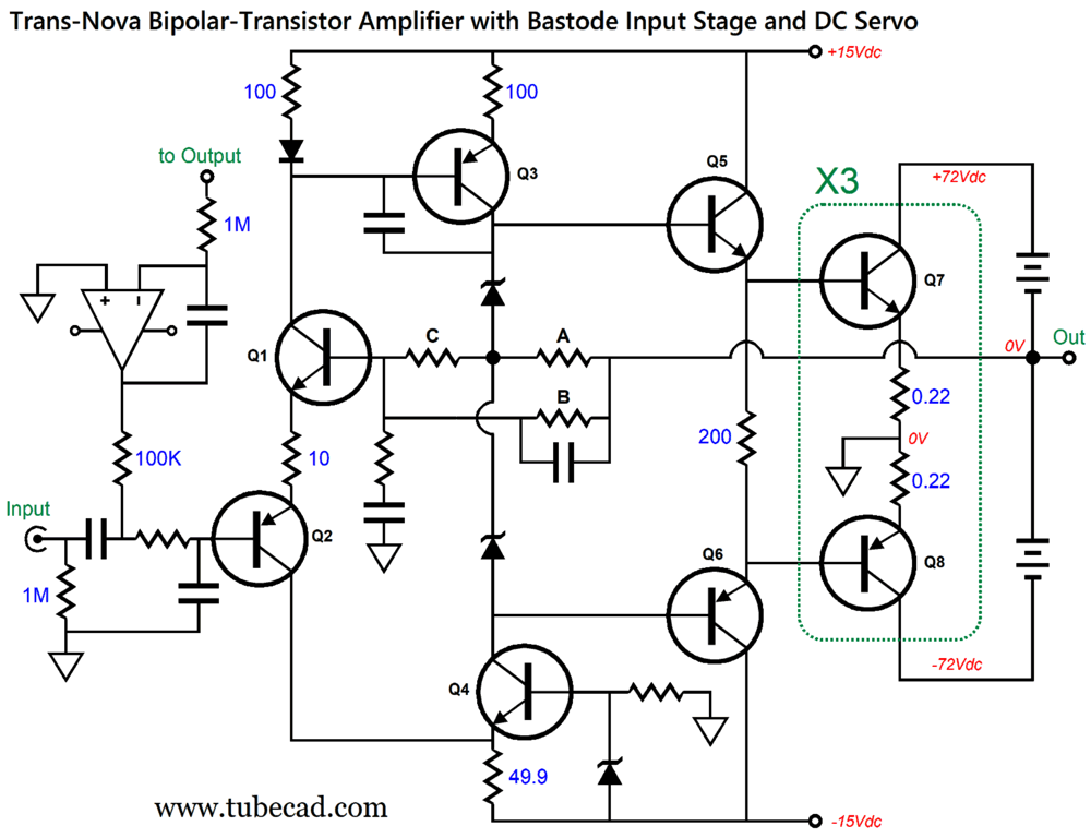
I remember reading the Acoustat white paper for their amplifier decades ago, but Google failed to deliver a link to it, sadly. After reading it, I instantly made a translation of the design into a tube-based equivalent, which took some effort, believe me. First, however, let's do a translation into bipolar transistors, which will require adding a few additional parts.
The 100-ohm emitter resistors improve the input transistors linearity. Transistors Q3 and Q4 were added to replace the zener in the original VAS circuit. Transistor Q3 and the diode form a current-mirror circuit that relays input transistor Q1's current conduction down to the 1k resistor at Q6's base. Transistor Q4 simply cascodes Q3 and probably is not essential. (With higher bipolar power supply rail voltages, it usually is needed.) By the way, the VAS stage still functions in a push-pull fashion still inverts its input signal at its output. Transistors Q7 and Q8 were added to drive the output transistors and to unload the VAS stage. The capacitor that shunts feedback resistor B is needed to ensure stability. (I didn't add the two needed Miller capacitors, aka Cdom capacitors, also needed to ensure stability, but I feared making the schematic too complicated.) The output transistors need to use emitter resistors to prevent current hogging. Unlike the lateral MOSFETs used in the Trans-Nova amplifier, which exhibit a lovely negative temperature coefficient, the bipolar output transistors exhibit a mad positive temperature coefficient. Indeed, the output stage could use some current-limiting circuitry, as bipolar transistors are not nearly as forgiving as MOSFETs. Another possible translation into bipolar transistors is the following:
(Damn shame that the RMAF ceased as this amplifier circuit would have made a fine entry in the private Annual RMAF Unanticipated Amplifier Challenge .) Translating the Trans-Nova into tubes runs into a snag: tubes only come in an N-version, with no P-version available. In other words, electrons only flow from cathode to plates, never the reverse. My workaround was to forgo the push-pull feature of the Trans-Nova's output stage and stick with single-ended operation.
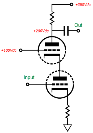
The input stage signal still enters a differential amplifier and a single triode functions as the voltage-to-current convertor stage, aided by the positive feedback from its plate to the input stage. Note that the output pentode's cathode is grounded and that the output transformer's primary DC resistance functions as a cathode resistor to cathode-bias the output tube; moreover, no negative power-supply rail is used. Also note that the pentode attaches to a floating 400V power supply, but its screen attaches the grounded fixed 350V power-supply rail. In other words, the pentode operates as pentode, not a triode-connected pentode. Three negative feedback loops are in place, each serving the same task as in the original MOSFET-based amplifier. What I like about this design, other than that 99% of tube-loving audiophiles and musicians will make no sense of it, is that feedback resistors A and B work to make the bottom of the output transformer's primary almost as ripple-free as its direct connection to ground. The clever thing to do is to choose feedback resistor C's value to zero the voltage at the connection with feedback resistor B. If the VAS triode's plate voltage is 250V, then feedback resistor C's value should be ten times that of feedback resistor B's value, as resistor B sees one tenth the voltage drop as resistor C. As I look over this circuit, I see the VAS stage in the middle as being the weakest link. One possible improvement might be to replace the grounded-cathode amplifier with a cascode amplifier.
The cascode topology offers higher gain and higher output impedance—both desired features for the Vas stage in this amplifier. Another, but far more complicated alternative is to cascade the input differential amplifier outputs into a second differential amplifier.
The MOSFET on the left acts as a capacitance-multiplier, the one on the right acts as compliant-constant-current source. Some may balk at the intrusion of solid-state devices, but the inclusion of the constant-current source already snuck some solid-state into the amplifier. (Of course, we could add a negative power-supply rail and create tube-based constant-current sources, after we replace the two MOSFETs with two triodes. This would work, but it would mean that we must use at least two heater power supplies, possibly three, due the huge voltage differentials between cathodes.) (I wish that I had written this post while Mr. Strickland was still with us, as I am sure he would have enjoyed seeing it. By the way, he designed the tube-based, high-voltage direct-coupled amplifiers for Acoustat.)
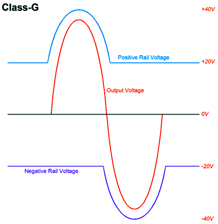
Class-G Trans-Nova Output Stage
Other than where the output is taken and where the ground connection is made, this topology is identical to that of a conventional source-follower output stage. Thus, the class-G operation works in the same fashion, in spite of the flipped ground and output connections. Why bother with class-G operation? Several reasons come to mind, all of them good. The first is that the main output MOSFETs Q1 and Q2 will dissipate much less heat at idle, as the voltage drop across them has been halved. Second, and certainly more important to me, is that we can mix technologies, using rare and expensive lateral MOSFETs for Q1 and Q2, and common, cheap, and vastly more powerful vertical MOSFETs for Q3 and Q4. The best of both worlds. At idle, the main output MOSFETs Q1 and Q2 draw their current from the center two 36V floating power supplies. As Q2 draws more current than Q1, the output voltage swings positive, as Q2 pulls up the string of floating power supplies positively. (Do not forget that this output stage inverts the input signal at its output.) Once the output voltage swing approaches +28Vpk, the commutating rectifier D4 is no longer forward biased, and rectifier D2 takes over, relaying the current flow from MOSFET Q2 to Q4, which allows the output voltage to further swing positively. When the output voltage swings negatively, it is due to Q1 drawing more current than Q2, with Q3 engaging, i.e. drawing heavy current, when the output voltage swings negatively beyond around -28V. My contribution to class-G operation is the addition of the 300-ohm resistor that bridges Q3 and Q4 sources. This resistor prevents Q3 and Q4 from ever turning off, which in turn prevents many headaches, such as those that arise from switching glitches and oscillation bursts. Does this mean that this is a class-A output stage? Good God no, as the main output MOSFETs Q1 and Q2 will turn off and Q3's and Q4's current conduction only gets relayed to the loudspeaker when the output exceeds ±28Vpk. I would actually use a different voltage split in the floating bipolar power supply, as music reproduction exhibits relatively low output voltage swings on average, with occasional big swings.
This floating bipolar power supply offers a nice 1-to-3 ratio between lower and higher voltages, as 72V is three time greater than 24V. The actual capacitor values and voltage ratings should differ, depending on the capacitor's location within the circuit.
When charged up, all the capacitors pack around the same amount of joules of energy. The assumption is that music playback is the amplifier's function, not shaker-table activation. If we want to add some overkill, we can use 10kµF/63V capacitors in place of the 4.7kµF capacitors.
Let's return to Acoustat's description of the Trans-Nova output stage:
Nice attributes, but why can't we derive the same features with a fixed, not floating, power supply? The alternative arrangement is simple enough:
The cascade of stage polarities remains the same: non-inverting, inverting, inverting. All three negative-feedback loops are still in play and still serve the same functions. Yet, a fixed (i.e. grounded, not floating) bipolar power supply is used, and it can feed two (or more) channels. As shown, the circuit won't work well without lateral MOSFETs, as the output MOSFET idle current will drift higher as the vertical MOSFET heat. The workaround is to replace the 5V zener with a transistor-based voltage-multiplier circuit that tracks the heatsink temperature change. Yes, the same circuit used in 99.999% of solid-state power amplifiers.
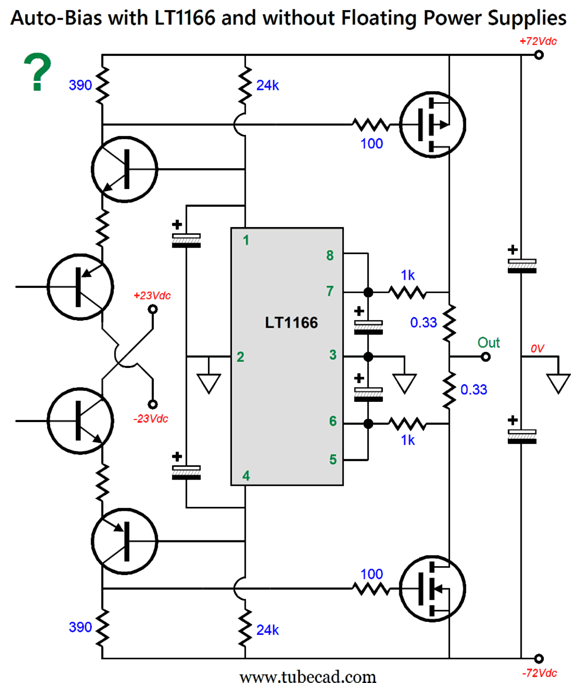
This got me thinking about the about the fantastically interesting auto-bias IC for MOSFET-based output stages, the LT1166.
I don't know for sure if this arrangement will work, thus the big question mark. Will the 0.33-ohm drain resistors ruin the otherwise low output impedance? The drain output impedance approaches infinity, so the addition of this trifling resistance makes no real difference; the amplifier's low output impedance is due to negative feedback loops A and B. A bigger potential problem is the voltage drop across these resistors, which will rob us of watts. The workaround is to shunt the drain resistors with low-voltage-drop rectifiers, such as a Schottky rectifier or an MUR420G. One last idea. Since the Trans-Nova amplifier's frontend can run off much lower power-supply rail voltages, why not use a high-quality OpAmp?
I don't know for sure if this arrangement will work, thus the big question mark. Will the 0.33-ohm drain resistors ruin the otherwise low output impedance? The drain output impedance approaches infinity, so the addition of this trifling resistance makes no real difference; the amplifier's low output impedance is due to negative feedback loops A and B. A bigger potential problem is the voltage drop across these resistors, which will rob us of watts. The workaround is to shunt the drain resistors with low-voltage-drop rectifiers, such as a Schottky rectifier or an MUR420G. One last idea. Since the Trans-Nova amplifier's frontend can run off much lower power-supply rail voltages, why not use a high-quality OpAmp?
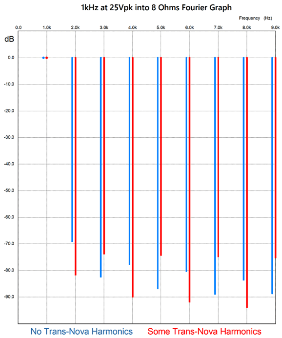
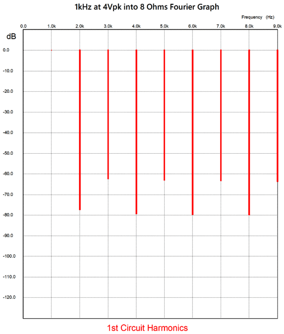
The previous design that retained the Trans-Nova negative feedback loop "A" produced a THD of 0.0394%, while the last design that forwent all the Trans-Nova features delivered 0.0409%, meaning that it seemingly lost the shootout. Why seemingly? I would much prefer to listen to this last design. Why? Look at the odd harmonics.
The previous design that retained the Trans-Nova negative feedback loop "A" produced a THD of 0.0394%, while the last design that forwent all the Trans-Nova features delivered 0.0409%, meaning that it seemingly lost the shootout. Why seemingly? I would much prefer to listen to this last design. Why? Look at the odd harmonics.
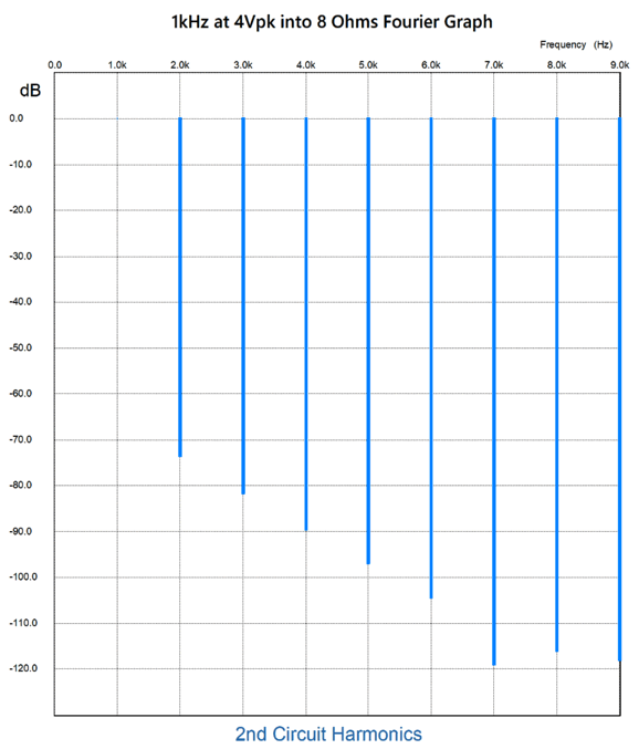
All harmonics are below -60dB, but the distribution favors greater suppression of even-order harmonics over odd harmonics. Typical solid-state power amplifier harmonic structure, in other words. Next, here are the last design's results, the one without any Trans-Nova flavoring.
Mercy, this is what I want to listen to, as the ear-lovely cascade of harmonics resembles that of a single-ended power amplifier. Note that the 7th harmonic is almost 120 dB down, compared to the 64 dB down of the Some Trans-Nova Attributes amplifier. This is not twice as good, but one thousand times better, as dBs are logarithmic units; each 20 dB difference is a tenfold difference. Why the difference? The extra negative feedback loop (A) in the previous design probably made for greater balance, hence greater suppression of even-order harmonics. (Or, possibly, just having two fewer transistors helped.) Does this say anything useful about the original Trans-Nova topology? Not really, as it is possible that the inclusion of its positive feedback loop undoes some of the forced balanced. I really need to run SPICE simulations on the original Trans-Nova amplifier. By the way, in my SPICE circuits, I used ±30Vdc bipolar power supply for the two output MOSFETs, which were IRF240 and IRF9240 types, not lateral types. In addition, we need to look at later development of the Trans-Nova topology, for example, in the Trans Nova Twin 120:
Note that the input stage differential amplifier now sports JFETs, not MOSFETs. Also note the inclusion fuses in the output stage. Later, Strickland joined Hafler and designed the Hafler 9300 power amplifier:
Note the complementary balanced/symmetrical input stage and VAS stage; also note the use of bipolar transistors and the cascoding. The output stage still holds lateral MOSFETs and floating bipolar power supplies.
Music Recommendation: Sienna Dahlen & Bill Coon, Balladextrous
//JRB
Did you enjoy my post? Do you want to see me make it to post 1,000? If so, think about supporting me at Patreon.
User Guides for GlassWare Software
For those of you who still have old computers running Windows XP (32-bit) or any other Windows 32-bit OS, I have setup the download availability of my old old standards: Tube CAD, SE Amp CAD, and Audio Gadgets. The downloads are at the GlassWare-Yahoo store and the price is only $9.95 for each program. http://glass-ware.stores.yahoo.net/adsoffromgla.html So many have asked that I had to do it. WARNING: THESE THREE PROGRAMS WILL NOT RUN UNDER VISTA 64-Bit or WINDOWS 7, 8, and 10 if the OS is not 32-bit or if it is a 64-bit OS. I do plan on remaking all of these programs into 64-bit versions, but it will be a huge ordeal, as programming requires vast chunks of noise-free time, something very rare with children running about. Ideally, I would love to come out with versions that run on iPads and Android-OS tablets.
|
I know that some readers wish to avoid Patreon, so here is a PayPal button instead. Thanks.
John Broskie
John Gives
Special Thanks to the Special 94 To all my patrons, all 94 of them, thank you all again. I want to especially thank
I am truly stunned and appreciative of their support. In addition I want to thank the following patrons:
All of your support makes a big difference. I would love to arrive at the point where creating my posts was my top priority of the day, not something that I have to steal time from other obligations to do. The more support I get, the higher up these posts move up in deserving attention.
If you have been reading my posts, you know that my lifetime goal is reaching post number one thousand. I have 406 more to go. My second goal was to gather 1,000 patrons. Well, that no longer seems possible to me, so I will shoot for a mighty 100 instead. Thus, I have just 16 patrons to go. Help me get there. Thanks.
Only $12.95 TCJ My-Stock DB
Version 2 Improvements *User definable Download for www.glass-ware.com
|
|||


| www.tubecad.com Copyright © 1999-2024 GlassWare All Rights Reserved |