| John Broskie's Guide to Tube Circuit Analysis & Design |
10 Aug 2009
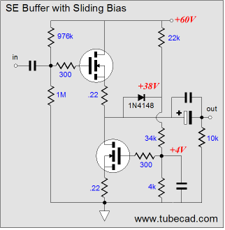
Although a regulated heater power supply would seem an unquestionably good idea, not everyone agrees. Some simply prefer AC on the heater elements, arguing that the AC heater voltage lends a mellow tone and retro sound that is much desired. I am not about to quarrel with fashion and taste preferences, but I am willing to argue that many have not heard DC on the heaters in the purest sense. For example, I have often employed motorcycle batteries to heat the heaters in test circuits that I have thrown together. Believe me—the battery truly improves the sound. Taking the heater’s transformer’s winding and rectifying it, however, is not the same. Why not? Using a big battery unloads the power transformer, whereas rectifying a winding only further burdens the power transformer; in fact, even more than just running AC into the heaters. How so? Rectification comes at a price, as rectifier voltage drops and capacitor heating subtract from the potential power. For example, a 12.6Vac/1.8A heater winding having gone through a full-wave rectifier circuit can no longer deliver 1.8A into the heaters. In fact, only about 1A is available. The math is simple, with a full-wave rectifier circuit, the maximum DC current output is equal to the AC-current rating divided by 1.8; and with a full-wave-center-tapped rectifier circuit, the DC current limit is equal to the AC-current rating divided by 1.2. In other words, many have “tried” DC by rectifying the heater winding, but they have also tried overtaxing the power transformer. For example, Dynaco was famous for making decent output transformers and using under-powered—sometimes amazingly under-powered—power transformers. Adding a heater rectifier circuit could easily throw the weak power transformer over the edge, thereby adding excessive power-supply noise and even grossly increased AC hum radiation due to the power transformer no longer being able to contain its electro-magnetic fields. Even when the power transformer is not over taxed, a rectified heater winding can cause problems. We all know that the bigger the power supply reservoir capacitor following the rectifiers, the lower the power supply ripple; but the bigger the power supply reservoir capacitor, the shorter the charging window, wherein the rectifiers can fill the large capacitor up. Because we can get away with low-voltage capacitor in the heater power supply, it’s not uncommon to find 10kµF and bigger capacitors being used. Thus, exceedingly small time apertures are created, wherein huge current inrushes must fill large capacitances in almost no time. These peak current conductions can easily couple to the other winding on the power transformer, as all the windings share a common core. On a scope, you can see the coupled current spikes on the B+ winding; and with your ears, you can hear them as an added scratchy texture. This is why I am always recommending using two power transformers, one for the heaters and one for the B+ voltage. Of course, using an external battery would bypass this potential problem. Well, the new power supply PCBs shown above are both sans heater power supplies and regulators. And they can be used when AC voltage is applied to the heaters or when an existing DC heater power supply is available; perhaps a big battery. I can see many adding them to existing tube gear, as the rectifier portion does not need to be used, if an existing rectified B+ voltage is in place. When will they be available for purchase? As soon as I complete my testing of the PCBs and finnish up the user guides.
Solid-State Email
Unity-gain power buffers are the hot item today, judging by my email. This interest is understandable, as a power unity-gain buffer can easily be mated to a vacuum tube line-stage amplifier, thereby creating a simple hybrid power amplifier. Ideally, no negative feedback loop would be required, but one could be added without too much extra labor. Many different designs have appeared here before; some of them obvious, such as the one shown above; and others more sneaky, such as the following.
For most solder slingers, the big question is whether to go single-ended or push-pull; and if push-pull, class-A or class-AB? But I see a secondary question for the push-pull output stage, symmetrical or asymmetrical drive? Asymmetrical drive usually results in dissimilar operation of the output devices, with one acting as the master device and the other the slave. Why bother with asymmetrical drive? It allows us to retain identical output devices, so we can more readily use two NPN transistors or N-channel MOSFETs, rather than search out NPN/PNP and N- and P-channel pairs, which are never matched as tightly as we would hope. (Strictly speaking, two NPN transistors or N-channel MOSFETs can also be used under asymmetrical drive, but just not as easily.) Once my mind began racing down this path, I thought of asymmetrical tube circuits, such as the SRPP and the Gomes amplifier. From here it was an easy jump to asking, "What would the Gomes amplifier look like if it were translated into silicon, say a solid-state power amplifier?"
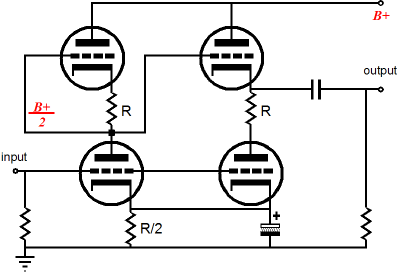
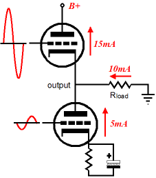
The Gomes amplifier has been covered here before. It belongs in the category of asymmetrical amplifiers, like the Transcendent OTL, the Murray, and Jeff Macaulay’s amplifier—all of which are push-pull amplifiers that hold matched pairs of identical output devices, but drive the output devices in an asymmetrical fashion. The Gomes amplifier may look similar to the Aikido, but it works in a much different way. For example, the Aikido’s output stage is a purely single-ended affair, whereas the Gomes is a push-pull configuration, albeit an asymmetrical push-pull setup.
The top-rightmost triode functions as a cathode follower, offering unity gain and low distortion and output impedance; in contrast, the bottom-rightmost triode functions as a grounded-cathode amplifier, delivering gain and a high output impedance. This may sound like a shotgun wedding; but it can work out quite well if the load resistance matches the Gomes’ tube and part value selections. In other words, for every actual physical instantiation of the Gomes amplifier, there is an optimal load impedance. And finding that optimal value is not difficult, if you are not afraid of simple math. In the Gomes amplifier, the input tube provides voltage gain for the output stage’s top triode, while its bottom triode sees the same input signal as the bottom input tube. The input signal will provoke fluctuations in the output stage’s bottom triode’s current conduction, white triode above it sees the input signal inverted and amplified; thus, the Gomes amplifier holds its own phase splitter and the output stage pushes and pulls into the external load impedance. Assuming that both cathode resistors in the input stage share the same value, the gain from the input stage will equal half the mu of the triode used; for example, a 12AX7 will yield a gain of 50; a 6SN7, 10; and a 6N1P, 17. Ideally, the cathode follower will deliver all the input stage’s gain into the load and that gain will equal the gain that the output stage’s bottom triode would develop working into the load impedance. In other words, the output stage’s bottom triode is configured as a grounded-cathode amplifier and it can deliver voltage gain as the load impedance is high enough. Now it gets a little tricky, as the output stage works in a push-pull, class-A fashion, the load impedance is effectively doubled. Doubled? When the bottom tube draws 5mA more current, the top tube draws 5mA less current, which means that the load sees a delta of 10mA, which will provoke twice the voltage drop across the load resistance that the 5mA change in current would seem to imply. Still doesn’t make any sense does it? Let’s add more details: at idle, both tubes draw 10mA and when the bottom triode’s conduction increases to 15mA, the top triode’s conduction drops to 5mA. If the bottom tube is conducting 15mA, 15mA must be flowing out of the tube and since the top tube is only conducting 5mA, the external must make up the difference.
In other words, since both triodes are in series, the only way the tubes current draw can differ is by having the difference in current conduction flow through the external load. No load, no difference. Under ideal conditions, the current swings between top and bottom triodes will be in perfect anti-phase, with one tube's conduction going up by the same amount as the other tube's conduction goes down. Imperfect anti-phase would be when one tube’s change in current conduction is not matched by the other tube’s inverted change current draw; for example, if the bottom tube’s conduction increases by 5mA, but the top tube’s conduction only decreases by 3mA. Equal current anti-phase swings result when the optimal load impedance is driven, which results when the output stage triode’s transconductance against twice the load impedance equals half the input triode’s amplification factor (mu). Expressed as a formula: Gm2Rload = mu/2 Solving for the load resistance gives us: Rload = mu/4gm Where gm refers to the output stage triode’s transconductance and mu refers to the input stage triode’s mu. As you can readily recognize from inspecting the formula, the greater the load resistance, the greater the input triode’s mu needs to be; and the greater the output stage triode’s transconductance, the lower the load impedance can be. Of course, these formulas are idealized, as they do not include the cathode follower’s gain loss or allow for unbypassed cathode resistor in the output stage, but they are—nonetheless—useful for getting close to the right load resistance. Now, let’s look at the Gomes amplifier’s output impedance. Note how the cathode follower provides the bulk of the hard work of keeping the output inline, while the bottom triode only offers up its plate resistance (rp) to buck perturbations at the output. Thus, the Gomes amplifier’s output impedance equals rp/(mu + 1) || rp, which reduces to rp/(mu + 2). In contrast, in a symmetrical push-pull output stage, both triodes would work equally at keeping the output impedance low, so the output impedance would equal rp/2(mu + 1), or half of what a single cathode follower would deliver.
Solid-State Transmogrification
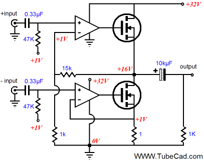
In the schematic above, we see our Gomes-amplifier inspired asymmetrical push-pull amplifier, complete with input and output stage. The OpAmps share the power supply rail as does the output stage and they drive and control the output MOSFETs. A differential input signal feeds the two OpAmps, so no phase splitter is needed.
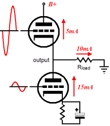
Note how the bottom MOSFET’s source follows the input signal and how that signal is superimposed on the 1-ohm source resistor. At idle, the source resistor undergoes a 1-volt voltage drop, which sets the output stage’s idle current to 1A, which limits the peak output current swing to 2A, which in turn equals 16W (RMS) and 16Vpk into an 8-ohm load (these are idealized values). The peak voltage drop across the source resistor is 2V and 0V sets the bottom limit. Thus, the bottom OpAmp and MOSFET define a current output amplifier, with no negative feedback extending from the amplifier’s output to the bottom OpAmp, so its output impedance is near infinite. In contrast, the top OpAmp and MOSFET are configured as a voltage amplifier. At idle the output voltage is set at half the B+ voltage by the ratio of feedback resistors and the +1V input bias voltage presented t the top OpAmp’s positive input pin. The feedback resistors set a DC and AC gain of 16, so the 1V bias voltage is amplified up to 16V. If this idealized asymmetrical amplifier is fed +/-1Vpk input signals, the bottom half will undergo +/-1A current swings, which the top half will meet with +/-1A anti-phase current swings, which in turn will yield +/-2A current swings into an 8-ohm load, developing +/-16V voltage swings across the 8 ohms. Thus, our implicit formula has been satisfied, as the amplifier bottom half presents a transconductance of 1A/V, which against 2R load equals 16, the fixed gain of the top half of the amplifier. The formula can be written as: Rload = gain/4Rsource Where Rsource is the bottom MOSFET’s source resistor (which assumes a 1Vpk input signal to drive the power amplifier to full output). If a 2-ohm source resistor were used, the load resistance would have to equal 16-ohms or the gain would have to be reduced to 8. Math, you've got to love it. Okay, what can be done to lose the differential input, as most of us do not run balanced systems?
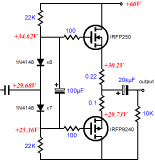
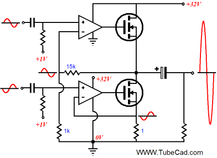
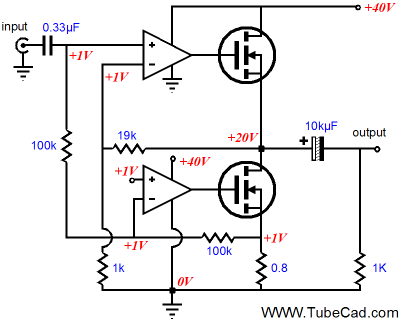
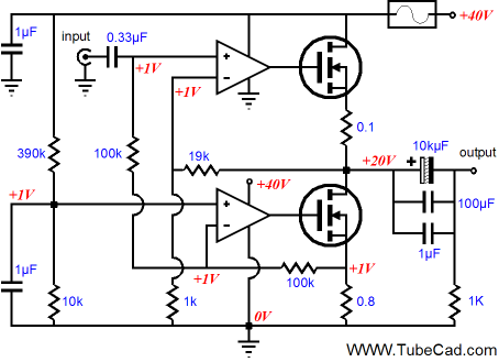
In the above schematic, we see a single, unbalanced input signal driving both OpAmps. The to OpAmp preserves the input signal’s phase and the bottom OpAmp inverts it; thus, there is no need for a differential input signal. A 1V reference voltage is needed to set up the desired idle current and voltage relationships throughout the amplifier. Note the increased B+ voltage, which reflects a move to actual from idealized. In addition, the source resistor has been decreased for the same reason. In other words, in order actually to get 16Vpk voltage swings into 8 ohms, our amplifier needs more voltage headroom, as the MOSFETs must see a greater positive gate voltage than their source sees to conduct. From the above schematic to the following one completes the journey to reality, as the following schematic shows the reference voltage, fuse, and needed coupling capacitor bypass capacitors. In addition, a 0.1-ohm source resistor has been added to the top MOSFET to improve its linearity and limit its maximum current conduction. What is missing, now that I look at it, is the gate-stopper resistors.
I know that many will grumble about the two coupling capacitors, the input and output capacitors. But I am at peace with them, as they allow for some sonic tuning (imagine PIO at the input) and the output coupling capacitor certainly makes for a much safer power amplifier. By the way, replacing the two-resistor voltage divider with a precision 1V voltage reference is not a good idea, as the resistors allow the amplifier’s output to always center, not matter how much the B+ voltage rises or falls; a fixed voltage reference would lock the output at exactly 20V, even when the B+ voltage exceed 50V or fell to only 30V. In programming, there is the trap of premature optimization; and in electronic design, there is a similar trap, the trap of excessive tweaking. Do not fall into it.
Conclusion
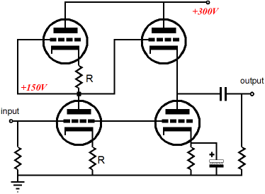
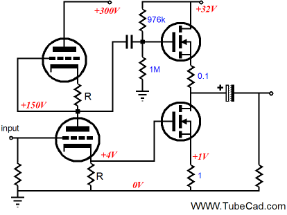
No OpAmps. The tube input stage provides both the voltage gain and the bias reference voltage for the MOSFETs. (Be sure to add grid-stopper and gate-stopper resistors and follow the formulas and run the triodes under high current, if you decide to experiment with this design.) A 6DJ8/6922 would develop a gain of close to 16 and the B+ voltage and cathode resistor value could be adjusted to attain the needed gate voltage for the bottom MOSFET (assuming a BUZ900 was used). Very interesting. By the way, I should point out that both mono Aikido PCBs now hold pads for diode biasing, so that a Moskido power amplifier can be more easily built.
In addition, both the octal and 9-pin mono Rev. D boards provide space for two equally large output coupling capacitors, which are also needed in a Moskido amplifier, which Bob Prangnell has discovered sounds best. See the following for more information on this hybrid topology: blog0058.htm
//JRB |
High-quality, double-sided, extra thick, 2-oz traces, plated-through holes, dual sets of resistor pads and pads for two coupling capacitors. Stereo and mono, octal and 9-pin printed circuit boards available. 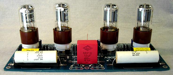 Aikido PCBs for as little as $24 http://glass-ware.stores.yahoo.net/
Support the Tube CAD Journal & get an extremely powerful push-pull tube-amplifier simulator for TCJ Push-Pull Calculator
TCJ PPC Version 2 Improvements Rebuilt simulation engine *User definable
Download or CD ROM For more information, please visit our Web site : To purchase, please visit our Yahoo Store:
|
|||


| www.tubecad.com Copyright © 1999-2009 GlassWare All Rights Reserved |