| John Broskie's Guide to Tube Circuit Analysis & Design |
09 April 2013
and
Solid-State Supercharger Review
The key idea here is that the tube does not work in parallel with the solid-state device, but in cascade with it, so the tube drives and controls the solid-state device, as any other arrangement would result in less tube flavor. In other words, we hope to impart the sonic signature of the tube, while obtaining the cost savings and ruggedness of solid-state devices. These goals might prove more difficult to achieve than we might have imagined, which I will dwell upon later. First, let's do a quick review of some possible hybrid topologies that give the steering wheel to the triode.
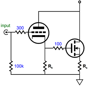
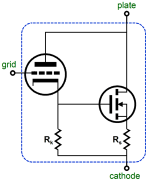
This is about simple as it gets. The triode drives the MOSFET's gate directly and as long as the source resistor (Rs) is much smaller in value compared to the cathode resistor (Rk), the MOSFET will provide the bulk of the current. The problem we face is that the cathode resistor may drop too much voltage, thereby overdriving the MOSFET; and a MOSFET, unlike a transistor, does not exhibit a perfectly predictable gate-to-source turn-on voltage. One workaround is the give the MOSFET its own bias-voltage network.
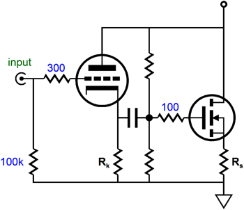
With this setup, the tube gets the cathode-bias voltage it needs and the MOSFET gets the gate-bias voltage it needs. Where it might get tricky is when multiple MOSFETs are placed in parallel; but the larger the Rs resistor value, the smaller the problem of current hogging will be. Why would we want to place several MOSFETs in parallel, rather than just one device? Heat, lots of heat. In a single-ended output stage, the output devices must draw a heavy current, which will in turn lead to high heat dissipation. And while a 150W power MOSFET would seem the perfect device for this hot application, reality disappoints.
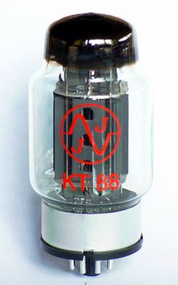
A power tube, such as a KT88, that boasts a 42-Watt maximum dissipation can actually be run with a 42W dissipation. It will not last nearly as long as it would with a 30W dissipation, but it won't melt down. A 150W power MOSFET, in contrast, would be hard pressed to dissipate a constant 42W in a real-life application. Why not?
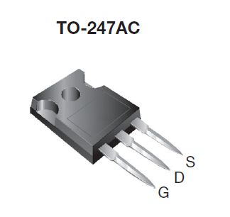
The 150W rating is derived from a quite atypical situation, wherein the MOSFET's case is held to a constant 25°C (77 degrees Fahrenheit), which would only be possible with an infinitely large heatsink made of solid silver or a refrigeration system. Under this uncommon cooling arrangement, the MOSFET's thermal resistance (between its junction and its case) and the temperature at which the junction will melt are the two limiting factors. For example, the IRFPG40, a 1000V/150W N-channel MOSFET, in the To-247AC package holds an Rthja (maximum junction-to-case resistance) of 0.83C/W and a maximum junction temperature of 150°C. Thus, if we can manage to keep the case temperature locked at 25°C and the IRFPG40 dissipates 150W (100V and 1.5A), then the junction temperature will be 150W x 0.83C/W, which equals 125°C, to which we must add the case temperature of 25°C, bringing us up to a total of 150°C.
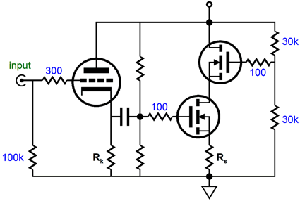
What if no heatsink is used with the IRFPG40, just as we wouldn't use a heatsink on the KT88? The IRFPG40's maximum junction-to-ambient resistance is 40C/W, which means that only 3.125W can be steadily dissipated in a 25°C environment, as (150C - 25°C)/40W = 3.125W. Not much is it? It would take fourteen IRFPG40 power MOSFETs with no heatsinks to equal one KT88 in terms of maximum heat dissipation. On the other hand, if we attach a large heatsink, the device could dissipate something much closer to its 150W rating. Except, and this is an important exception, that since heatsinks are usually fitted to the outside of the power amplifier chassis (at least with high-end gear), the heatsink can be readily touched by you or by a child or by a pet. My own maximum limit on heatsink temperature is 60°C (140°F), which will be far too hot to hold, but not hot enough to burn your skin off. This self-imposed limit will make dissipation calculations a bit harder and it will further limit the maximum dissipation the MOSFET can steadily undergo. For example, we must subtract the temperature next to the heatsink, which might be a low 20°C in a cold basement, but might be a high 30°C in the summer or with hot tubes and power transformers nearby. In addition, heatsinks are measured in the middle of the room, as they hang by a string, not crammed in a small electronics enclosure. Moreover, a layer of dust will add to the heatsink's thermal resistance. Assuming the textbook 25°C, however, leaves us with 35°C, which means that the MOSFET's dissipation cannot be any more than what will add the additional 35°C of heat to the heatsink's dissipation. Well, how does one figure out that value? Heatsinks present a thermal resistance, which is measured in degrees C per watt. A big, massive heatsink might present only 0.5C per watt, whereas a small heatsink could present as much as 3.5C per watt. In either case, we divide the 35C by thermal resistance, so the big heatsink's mere 0.5C per watt resistance would allow 70W of dissipation from the MOSFET, assuming that its junction temperature didn't exceed its limit. The small heatsink, in contrast, would allow only 10W of dissipation from the MOSFET. Read Burr-Brown's Application Bulletin SBOA021 for more information. All of this argues for using more MOSFETs, as each device will be asked to dissipate less heat and several devices can be spread along the length of a long heatsink, increasing the heatsink's cooling ability by sidestepping hotspot creation. Normally, the MOSFETs (or bipolar transistors) are placed in parallel, but his arrangement adds its own difficulties. For example, most power MOSFETs present a fairly high input capacitance, which can only increase as more devices are placed in parallel. One workaround is to place the MOSFETs in series, as shown below.
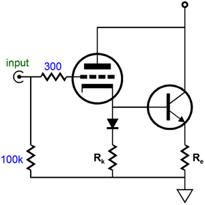
Each MOSFET sees half the voltage and each dissipates the same amount of heat, but the input capacitance is the same as a single MOSFET. Actually, the situation is a bit better than that, as the triode only has to drive half the Miller-effect capacitance that it would face with a single MOSFET. (This arrangement works well with high-voltages and low currents, but not that well with low-voltages and high currents.) Let's now look at some bipolar transistor topologies. The following design uses the diode to cancel the base-to-emitter voltage drop within the transistor, ensuring that resistors, Rk & Re, see the same voltage across their leads.
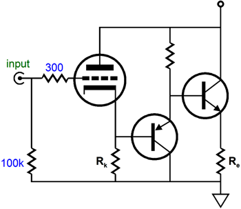
Since resistors Rk & Re see identical voltages across their leads, the ratio between their values also equals the ratio between their current conduction. Thus, if Rk is three times bigger than Re, the transistor will pass three times as much current as the triode ( we can ignore the current flow into the transistor's base). Another approach is to replace the diode with a PNP transistor, which also undo the base-to-emitter voltage drop in the output transistor and will unload from the triode the task of driving the output transistor's base.
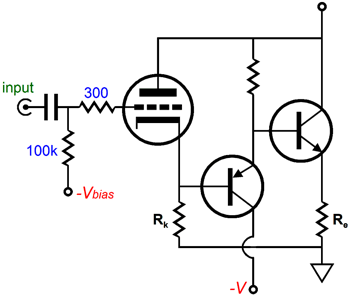
One problem this half-a-diamond topology may give rise to is too little voltage across the PNP transistor to allow it to fully turn off the NPN transistor. Indeed, it would be far better to give the PNP transistor's collector more voltage to work with. And there's the problem the triode requiring a fairly high cathode voltage, which will just waste heat in resistors Rk & Re. The following variation fixes these problems.
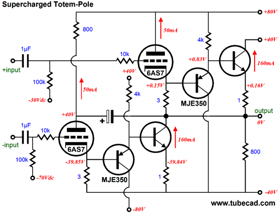
Note how in each of these circuits the triode's plate is connected to the MOSFET's drain or the transistor's collector. This is an essential part of the current supercharging concept, when the load attaches to the plate that is, as the triode's rp (plate resistance) will function as a negative feedback loop of sorts to further keep the triode in charge of the solid-state device. If the solid-state device draws too much current, the plate voltage will fall, which will cause the cathode to fall 1/mu, where mu is the triode's amplification factor, thereby causing the solid-state device to ease up on its conduction. Remember that there are three ways to control a triode's current conduction: change the plate voltage, change the grid voltage, and change the cathode voltage. The most effective of the three is changing the cathode voltage, as it is mu + 1 times more effective than the same voltage change at the plate. The second is changing the grid voltage, which is mu times more effective than the same voltage change at the plate. And, finally, changing the plate voltage. On the other hand, if the load attaches at the cathode end of the triode, then the triode's plate and the solid-state device's collector or drain need not connect. Effectively, they do connect in AC terms through their connections to their B+, which should offer near zero impedance. Thus, the following supercharged design shows the two configuration well, as the top triode and its output transistor see the load at the triode’s cathode, so the plate and collector can attach to separate power-supply B+ connections; and as the bottom output transistor see the load at the output’s transistor’s collector, the large-valued electrolytic capacitor must be used to tightly couple the plate to the load.
In the above schematic, the electrolytic capacitor’s value is not marked, but it should be large enough to ensure that the bottom 6AS7 triode’s plate is effectively coupled to the external load, say 300µF to 1kµF. (Of course, this capacitor could and should be bypassed by a film or PIO capacitor.)
Some Supercharged SE Amplifier Examples In addition, 330Vdc is about what we get when a 230Vac to 240Vac secondary is rectified. Moreover, 400V capacitors are readily available, whereas 450V and 500V capacitors are much harder to find. In strict observance of the universal Law of No Free Lunches, I must point out that if we lower the B+ voltage, then we must increase the idle current, if we hope to achieve the same power output. And with a lower B+ voltage and higher idle current, we will need to find an output transformer with a low winding ratio and, thus, a low primary impedance.
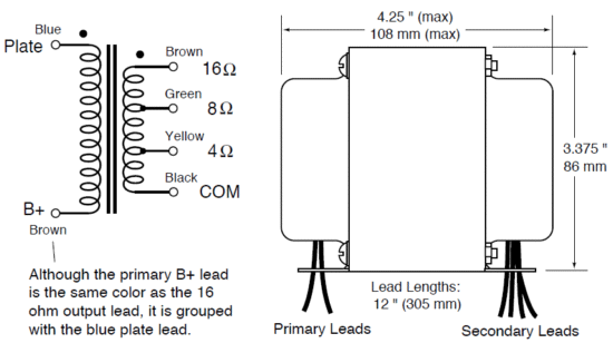
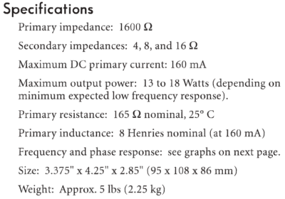
I have mentioned the One Electron output transformer the UBT-1 many times before, which makes sense, as I just love this transformer. Love? Oh yes indeed, love; I so esteem this transformer that I own six of them. After decades of putting square waves into an output transformer’s primary and seeing garbled sort of square waves come out of it secondary, I realized that, in general and with few exceptions, the higher the winding ratio, the worse the waveform out of the secondary. Here is an extreme example: I once found a beautifully made transformer at an electronic-surplus store with a $1 price tag, so I bought on a whim. I tested it and discovered that it held a 1.414 winding ratio, no doubt so that easy AC square root of 2 divisions could be performed in an analog fashion. I then tested the mystery transformer with square waves. At first I thought I must have hooked the scope’s probes up to the signal generator’s output, as a perfect square wave traced across the scope’s screen. I hadn’t. Of course, 1:1 isolation transformers get an added cheat due to the intra-winding capacitance helping improve the high-frequency performance and this transformer was close to 1:1, so I placed a high resistance in series with the primary and I loaded the secondary with a low resistance that would sidestep the capacitance cheat. It's output still looked beautifully square. Well, the UBT-1 holds a 14:1 winding ratio, so it reflects the 8-ohm load to its primary as 1600 ohms, very low indeed. With an idle current of 150mA, the UBT-1 output transformer will put out about 16W. Remember that I² x Rload/2 = W, where W is the real average wattage, not the advertising peak wattage.
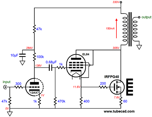
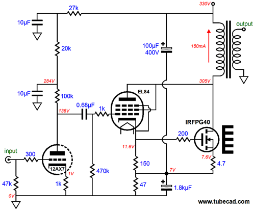
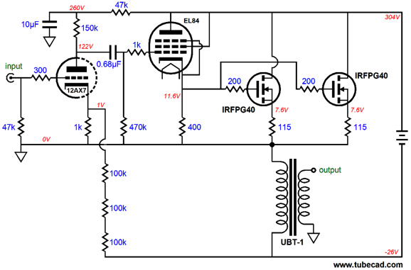
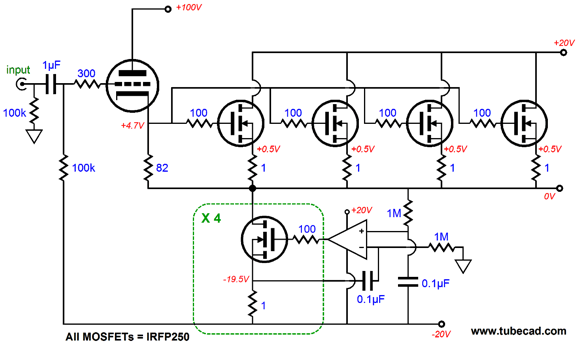
Because we start with a 330V B+ voltage, we can use an EL84 (6BQ5), which is a wonderful little tube, being easy to drive and quite robust. The above single-ended amplifier design uses an EL84 cascading into a high-voltage MOSFET, the IRFPG40. The EL84 is triode connected and its cathode is DC coupled to the MOSFET’s gate. Since resistor Rs is so much smaller in value than the tube’s cathode resistor, the MOSFET will conduct the bulk of the current at 120mA, whereas the EL84 will only conduct 30mA. Wait a minute; the MOSFET’s source resistor is 6.66 times smaller in value than the cathode resistor, so why doesn’t the MOSFET draw 6.66 times more current? It would, if both resistors saw the same voltage drop, but they don’t, as the cathode resistor sees 4V more voltage than the source resistor. As I look at this amplifier schematic, I am just itching to modify it. Not that it is a bad design. Indeed, it is at least as good as many high-end boutique audio products. What troubles me is the poor PSRR of the amplifier. As shown, no negative feedback loop extends to the output transformer’s secondary, which would work to improve the PSRR—nor would I be eager to add a global feedback loop. (The amplifier’s high gain is a feature in an integrated–amplifier, which forgoes the need of a line-stage amplifier. And adding a feedback loop would necessarily decrease the gain.) Before showing my solution to the poor PSRR, I want you to abstract out of the schematic the following electronic meta device, which consists of the triode-connected EL84 and the power MOSFET.
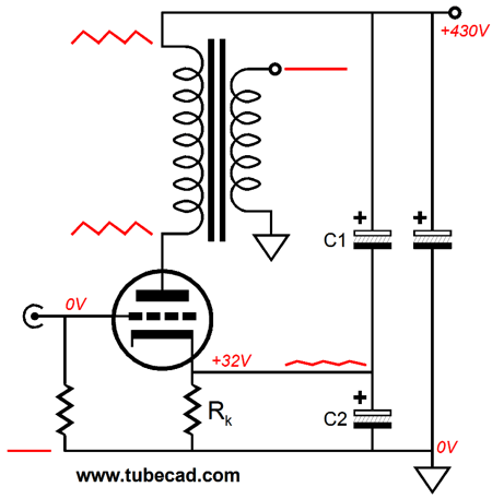
Next, use this hybrid device in my Aikido-esque noise-canceling scheme that I revealed here back 1999, which purposely injects a sampling of the power-supply noise into the output tube’s cathode, thereby causing a null in power-supply noise on the output transformer’s secondary. The idea behind this technique is simple enough: if the power-supply noise doesn’t prompt a variation in current conduction by the output tube, the output transformer’s primary cannot see the power-supply noise, so the transformer cannot relay the noise to its secondary.
In the above schematic, capacitors, C1 & C2, perform the needed voltage division on the power-supply noise. Well, a similar setup can be added to our supercharged single-ended amplifier.
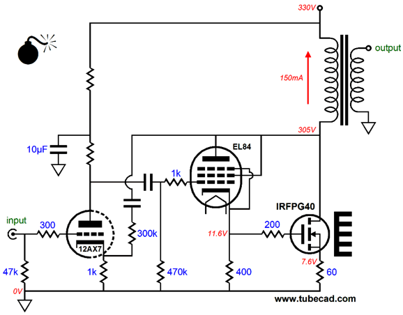
The 100µF/400V capacitor is 1/mu times as big as the 1800µF/16V capacitor below it. The 47-ohm resistor is common to both the EL84 and the IRFPG40 and functions as a shared cathode-bias resistor. This arrangement yields a huge improvement in PSRR. In addition, the two RC filters that feed the 12AX7-based input tube also help. Of course, adding negative feedback loop that would extend from the 12AX7’s cathode to the output on the secondary would also help improve the PSRR and lower both the distortion and output impedance, but danger lies in the phase shift that the output transformer must introduce. In other words, add the feedback loop only if you are bold and you know what you are doing. On the other hand, if we added a negative feedback loop before the output transformer, the output transformer’s squirreliness would be sidestepped. A great idea, but there’s one problem, a big problem.
The problem with the above circuit is that it will worsen the PSRR, not improve it. The negative feedback loop will strive to ensure that no power-supply noise appears at the EL84’plate, which seems like a worthy goal—and it would be, if the output were taken at the EL84’plate, but the output is taken from what appears across the output transformer’s primary. In other words, this arrangement ensures that the PSRR will fall close to zilch, which is not good. In contrast, if the output transformer terminated into ground, rather than the B+ connection, then the negative feedback loop would work to improve the PSRR. But how would that be possible? Well, if you just asked yourself that question you are not a long-time reader of the Tube CAD Journal. The workaround is the inverted single-ended-amplifier topology.
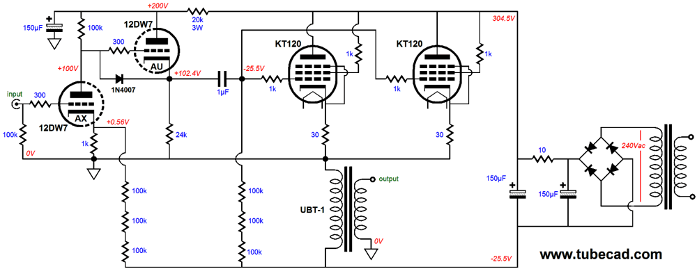
Supercharged Inverted Single-Ended Amplifiers
I decided to use two power MOSFETs this time, as I worried about excessive dissipation from a single MOSFET. But everything else is quite similar: the same power supply voltage the same input and output tubes, and the same idle current and power output. The three 100k resistors in series complete the feedback loop that extends from the 12AX7’s cathode to the bottom of the output transformer’s primary. Why three resistors and not one 300k resistor? Resistors give rise to voltage-induced distortion, which three resistors will lessen. In addition, bottom lead of the output transformer’s primary will undergo +/-225Vpk swings which only produce 84mW of heat in a 300k resistance, but some audiophile-grade resistors are high-voltage phobic, such as the famous old HolCo resistors, so letting each 100k see only +/-75Vpk of voltage swing is safer. By the way, do not make the mistake of believing that it is some magical property of the solid-state supercharging that all us to invert the single-ended amplifier topology, placing the output transformer below the output tube. An all-tube inverted single-ended amplifier is just as possible, as the following schematic shows.
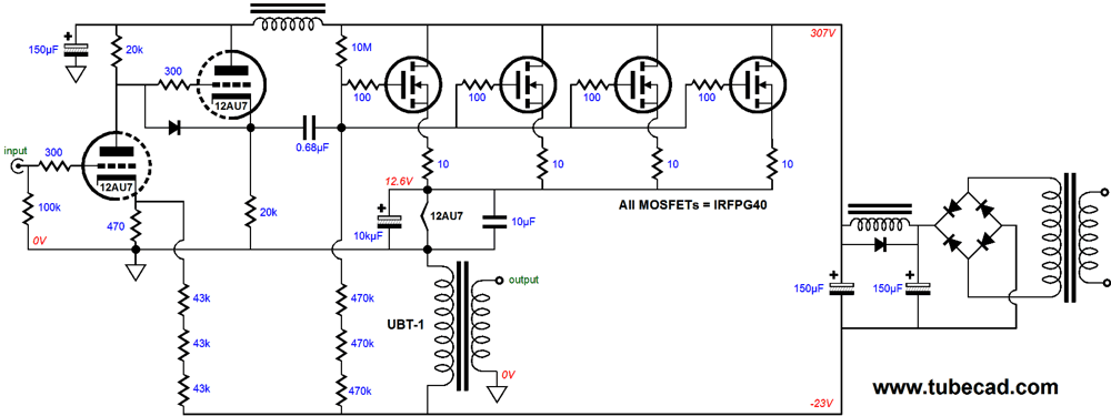
Note that the 20k RC filter resistor is effectively in parallel with the output transformer’s primary, which means that this resistor will see the +/-225Vpk voltage swings, which in turn means that its will dissipate a lot of heat at full output. One workaround is to replace the resistor with a choke. Ideally, an inductor displaces no DC voltage and dissipates zero heat. In reality, chokes are made from wire, which means that the wire’s resistance prevents both claims from being true. Nonetheless, a good choke would present only a fraction of the 20k resistor’s resistance, so it is certainly close enough to ideal. Here is an interesting possibility, a hybrid inverted single-ended power amplifier that uses the 150mA idle current through the four power MOSFETs to heat the 12DW7’s heater. Not a free lunch, as we will lose 12.6V of B+ voltage, more of a free snack.
True enough, no solid-state supercharging takes place in the above hybrid inverted single-ended power amplifier. Still, I would love to hear such a beast. Why four power MOSFETs? I just performed some quick math, which revealed that four IRFPG40 MOSFETs would just make it under the wire, in terms of heat dissipation, with a 2.6C/W heatsink per device.
Big heatsinks are expensive and rare, whereas the tall heatsinks that I provide in my kits are relatively cheap and plentiful. Oh, so many ideas and so little time. A curse…or is it a blessing? Who knows. Speaking of too many ideas, the following will be my last circuit, as this post is getting too long. (By the way, I often get e-mail that goes like this: Why don’t you… show this… design that… talk about a different… review it… explicate something that I am interested in… use more 2A3s… You get the idea. Well, if you are tempted to send me such an e-mail, why not create your own blog, draw your own schematic, write your own verbiage, and post it yourself and then send me the link, as my fingers and mouse could use a rest. ;) The idea here is that not all single-ended amplifiers need an output transformer, as directly coupling and a constant-current source can be used. The obvious downside to a constant-current-source-based design is the twice the heat is dissipated and a maximum efficiency of only 25% can be realized. Mind you, that was a maximum theoretical efficiency, so expect reality to come in at closer to 15-20%. Below, we see a 6C19C noval power triode from Russia supercharged by four power MOSFETs.
The idle current is a heavy 2A, so 16W is possible into an 8-ohm load. Eight power MOSFETs are used per channel and half are used as source followers, while the other half make up the constant-current source. A high-voltage OpAmp, such as the LF411, controls the bottom MOSFETs and ensures a low DC offset at the output, not a fixed idle current. What! This circuit is what I call a compliant-current source, not a constant-current source. If the triode and its slave MOSFETs conduct 2.2A, the OpAmp will make sure that the bottom MOSFETs also draw 2.2A, as only that value will establish a 0V output at idle. The solid-state rail voltages and triode’s B+ voltage are not unrelated, as they assume the use of a PS-6 power supply.
The PS-6 power supply presents three output voltages: a low-voltage bipolar output (up to +/-50Vdc) and a voltage quintupled high-voltage B+ output voltage roughly equal to five times the bipolar rail voltage. For example, if the rail voltages are +/-30V, the high-voltage B+ output will be about 147Vdc; if the rail voltages are +/-20V, the high-voltage B+ output will be about 98Vdc. This single-ended supercharged power buffer offers a gain of around 0.7, so an input signal of 24Vpk will be needed to bring the buffer to full output. Well, where is this signal gain going to come from? If you own a hot tube-based line-stage amplifier, you may already have the solution. Failing that, I would use an Aikido gain stage with the same 100V B+ voltage the 6C19C uses; a 12AT7 input and output tube would yield a gain of about 30, which would be plenty. Oh, so many ideas and so little time. Definitely a curse, the more I think about it.
Next Time
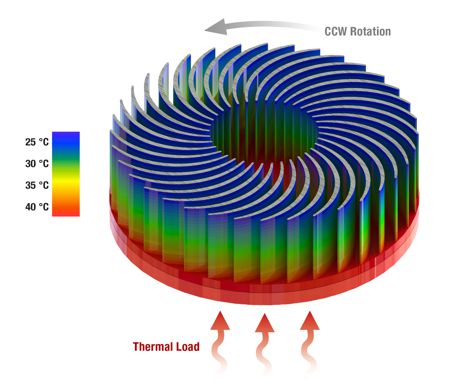
*Heatsink Developments The second development is by Sandia National Laboratories, which has invented and rotating heatsink—well, the top half spins—that they call a “Air Bearing Heat Exchanger.” Cool, no?
I have often said that audio lives off the crumbs that fall off the technology table. The 300B was not designed with audiophiles in mind, nor was high-end audio a consideration in the creation of bulk-foil resistors, soft-recovery rectifiers, Teflon capacitors, nor was just about every component you can buy from Mouser or Digikey. Well, eventually, we will see these fancy heatsinks used in high-end audio gear, whose glossy ads will imply that the audio company itself had created the technological wonder, not just appropriated it.
//JRB |
I know that some readers wish to avoid Patreon, so here is a PayPal button instead. Thanks.
John Broskie
Kit User Guide PDFs
And
High-quality, double-sided, extra thick, 2-oz traces, plated-through holes, dual sets of resistor pads and pads for two coupling capacitors. Stereo and mono, octal and 9-pin printed circuit boards available.
Designed by John Broskie & Made in USA Aikido PCBs for as little as $24 http://glass-ware.stores.yahoo.net/
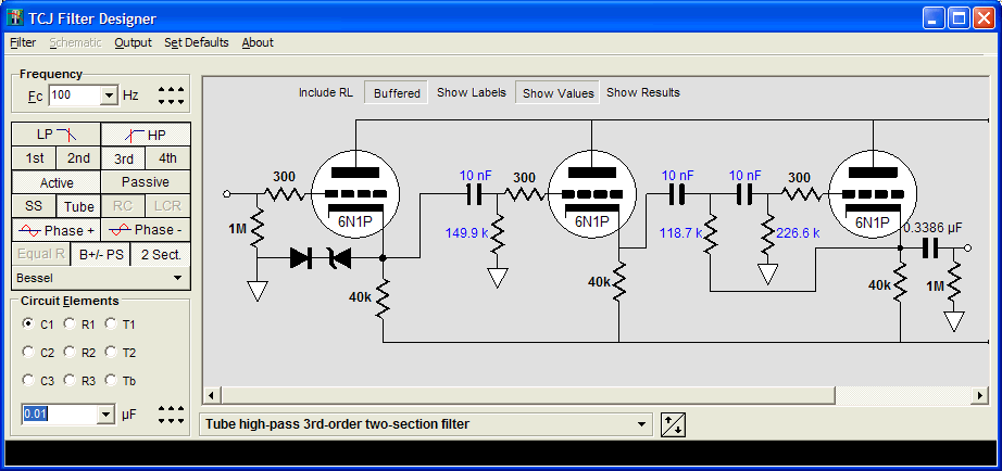
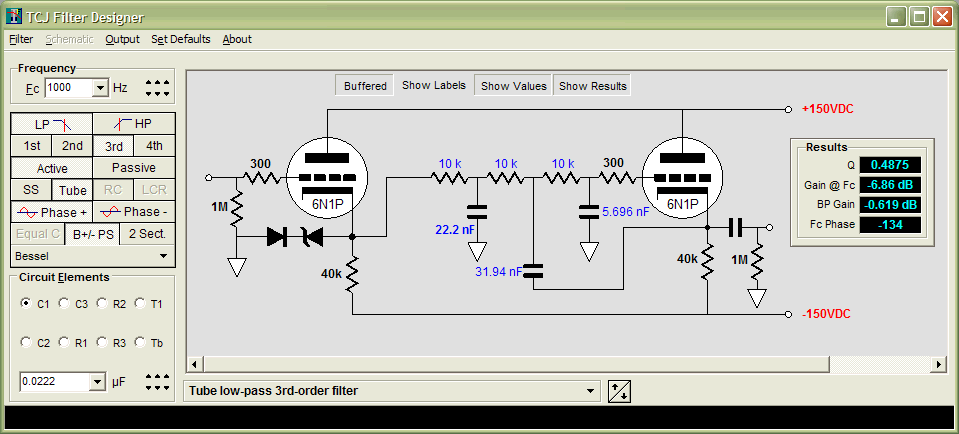
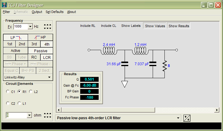
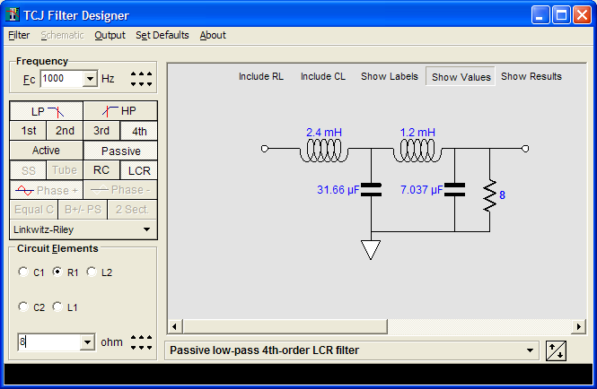
The Tube CAD Journal's first companion program, TCJ Filter Design lets you design a filter or crossover (passive, OpAmp or tube) without having to check out thick textbooks from the library and without having to breakout the scientific calculator. This program's goal is to provide a quick and easy display not only of the frequency response, but also of the resistor and capacitor values for a passive and active filters and crossovers. TCJ Filter Design is easy to use, but not lightweight, holding over 60 different filter topologies and up to four filter alignments: While the program's main concern is active filters, solid-state and tube, it also does passive filters. In fact, it can be used to calculate passive crossovers for use with speakers by entering 8 ohms as the terminating resistance. Click on the image below to see the full screen capture.
Tube crossovers are a major part of this program; both buffered and un-buffered tube based filters along with mono-polar and bipolar power supply topologies are covered. Available on a CD-ROM and a downloadable version (4 Megabytes). |
|||


| www.tubecad.com Copyright © 1999-2013 GlassWare All Rights Reserved |