| John Broskie's Guide to Tube Circuit Analysis & Design |
31 October 2015
Class-A? Class-AB?
Class-A: The Gold Standard
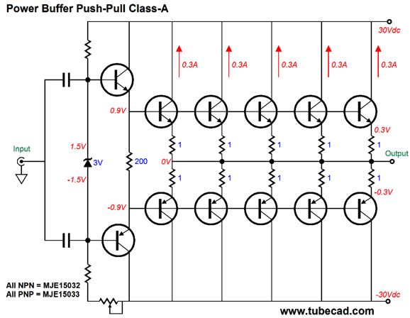
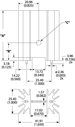
What! Is that it? Where is the interesting stuff? First, half of the interesting stuff is not shown, as the heatsink does not appear in most schematics. But in this circuit, it is of key importance. Second, only two types of transistors are used, the MJE15032 and MJE15033. These are 250V, 8A, 50W complementary power transistors in a TO-220 package with an Ft of 30MHz. Usually, they are not used as output devices, but as driver transistors. They cost a little over a $1 each, which means that all 12 of them in one channel will cost less than one decent power tube. Class-A means heat, lots of it. The ten output transistors idle at 300mA each, so a total of 1.5A of idle current per channel, which means 90W of heat dissipation at idle as 1.5A x 60V = 90W. That is a lot heat and getting rid of it is not easy. Let's do some simple math: if we set an upper limit to the heatsink's temperature to 60C, and if the ambient temperature is 25C, then we can only allow the heatsink to climb in temperature by 35C. This means that the heatsink must only get 35C hotter with 90W of power being radiated. Thus, the heatsink's thermal resistance must be no more than 35/90 or 0.39C/W, which implies a big, heavy, and expensive heatsink. Or does it? What if we give each of the 10 output transistors its own smaller, lighter, cheaper heatsink? What if we use ten separate heatsinks with a thermal resistance of only 2.6C/W? The ten separate 2.6C/W heatsinks effectively equal one 0.26C/W heatsink, as all the thermal resistance are effectively placed in parallel.
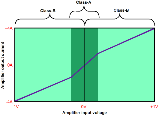
The result would be impressive. Think about it: a phalanx of two by five heatsinks, each standing 2.5 inches tall, all placed on a 6 by 12 inch PCB. The closest tube analogy might be imagining ten EL84 output tubes running in class-A, push-pull. (By the way, I think that using ten EL84 tubes per channel is a great idea.) Indeed, the ten discrete heatsinks would somewhat resemble ten tubes. Assuming an insulator resistance of 1C/W, combined with the transistor's 2.5C/W and the heatsinks' 2.6C/W resistances, each heatsink would only become 48.4C hot (with an ambient temperature of 25C) and the all-important transistor junction temperature would be only 80C, far below its 150C limit. Understand that 25C translates to 77 degrees Fahrenheit and that if the actual temperature inside the chassis is closer to 35C (95 F), then each heatsink will be 58.4C hot and the junction temperature will be 90C hot. On the other hand, the nice thing about class-A operation is that, unlike a class-AB amplifier, as power is being delivered into the speaker, the class-A output stage cools. Still, class-A operation requires plenty of ventilation. How much power could this circuit deliver? Before we can answer this question, we need to know the load impedance. Assuming an 8-ohm load, this power buffer can swing twice its idle current value into the 8-ohm load, so 3Apk is the peak current swing, which implies an output wattage of 36W, as I² x R/2 = W. Amazing isn't: we needed to use ten 50W devices to get 36W of class-A output. If we used the MJL21193 and MJL21194 pairing instead, we would still only get 36W, but the transistor junction temperatures would run cooler, due to the TO-264 package's lower junction-to-case thermal resistance, only 0.7 C/W. What if a 4-ohm speaker is driven instead? The class-A window of operation only allows 18W of class-A power, but 72W of class-AB watts might be summoned, if the power supply can sustain the higher current demand. Class-A operation is bounded by current flow, not voltage swings. If this class-A buffer delivers more than 3A of current, then it is no longer operating in class-A. If we raised the idle current by the squareroot of 2, i.e. 1.414, or 2.12A, then the buffer could deliver 36W of class-A power into 4-ohm speakers, but the rail voltage would have to be reduced by the same 1.414 factor, i.e. +/-21.2Vdc. This would prove a pain, as custom-made power transformers would be required and as would a means of switching bias voltages. And here lies the problem with this design: many people own 4-ohm speakers. In addition, even if your speaker is nominally an 8-ohm design, its impedance may fall far below 8 ohms at some frequencies. Once the top five NPN output transistors exceed double their idle current flow, the bottom PNP output transistors will cutoff, which means that the output stage will depart class-A and enter class-AB, albeit a very rich class-AB. Isn't that a good thing? No, not really, as we run into the problem of gm doubling. In class-A operation, the buffer's output impedance is about 0.1 ohms, which implies a damping factor of 80; but in class-AB, 0.2 ohms, which implies a damping factor of 40.
The Problem of gm Doubling The club of knowing members is small. (Just as the beautician and hairstylist are not invited into the plastic surgeon's operating room, accomplished part-swappers are not invited to these club meetings. No amount of expensive parts will solve this problem.) One member in good standing is Robert Cordell, who does extensively cover the topic in his masterful book, Designing Audio Power Amplifiers. Another member is Douglas Self, who brings up the topic at least twice in his essential book, Audio Power Amplifier Design Handbook. The second reason the topic fails to achieve liftoff is that those few who do know about it usually take one of two positions: the first point of view is that much like poor, which—as we have been told by a reliable source—we shall always have with us, gm doubling is an intractable problem that we must live with, as no solution other than more negative feedback is available; or second, they hold that while it is true that gm doubling occurs, it is not that big a deal, as an optimally lean idle current (a nearly class-B biasing of a class-AB output stage) effectively cancels out the doubling of transconductance (this is Self's and W. Marshall Leach, Jr's position); others point out that the bigger the loudspeaker's impedance is, the smaller of a problem gm doubling becomes, as the higher load resistance greatly mitigates the output stage's transconductance, making the current conduction overlap far less of an issue, certainly nothing that more negative feedback cannot iron out. As you (no doubt) might expect, I take a different stance, as I believe that gm doubling is a much bigger problem than most imagine and I believe that it can be overcome. Indeed, the answer is obvious: we simply need to design constant-transconductance output stages.
Before digging any deeper, let's pause and reflect that we have all heard constant-transconductance output stages before, as we have all heard single-ended and class-A push-pull amplifiers, both of which contain constant-transconductance output stages. Think about it: a single output tube (or MOSFET or transistor) presents its transconductance throughout the output waveform being produced. And two tubes or solid-state output devices running in honest-to-God class-A, push-pull operation will also present their two transconductances in parallel throughout the output waveform; thus effectively doubling the single device's transconductance even at full output. Do these two types of power amplifiers enjoy good reputations for good sound? Of course, they do. Class-AB output stages, on the other hand, may be advertised as sounding as good as a single-ended and class-A push-pull amplifiers, but reality sadly disappoints. As does the obvious but bad choice of running an extra rich idle current, so that there is more class-A in the class-AB blend*. Alas, like so many obvious fixes, such as imposing $40 an hour minimum wage or low-res MP3 files, the fix just begets bigger problems. (On the other hand, I suppose that truly crazy rich idle current, say one that produced 20W of class-A power in a 50W class-AB power amplifier might not sound too bad, as the transitions into class-B would occur at so high a volume level that our ears would already be too stressed to really notice any extra discontinuities in the sound.)
Okay, I better backup further. The problem of gm doubling lies in the discontinuity in transconductance and in output impedance in a class-AB power amplifier's output waveform, as the amplifier shifts from class-A to class-B. At idle and up until the output stage departs from class-A operation and enters class-B mode, the two active output devices combine their transconductance, hence the term, “gm doubling.” With only one output device active, the gm halves and output impedance doubles, and the eternal load effectively appears to halve in resistance. Since both output devices enter and exit class-A, two discontinuities result near the transitions from positive to negative output voltage swings. The ear hears these sonic speed bumps and complains, much like your hand encountering cracks in an otherwise smooth surface. Whatever other faults that single-ended and class-A push-pull amplifiers may suffer from, these amplifiers do not bump in the middle.
Frederick Nietzsche profoundly pointed out that the more abstract the concept, the more one must seduce the senses to it. Thus, I have sought a good analogy. The best that I have come up with is the following. Imagine that you own a movie theater and that you want to show wide-aspect films, which your wide screen can accommodate, but which your old projector cannot, as it projects a nearly square image. One workaround would be to use two projectors, with each getting half of the horizontal image, so one would project the right half of the wide-screen film, while the other projected the left half. Great care must be exercised in aligning the two images, so no gap shows. Unfortunately, a perfect alignment proves difficult to achieve and difficult to maintain, as footsteps and road traffic shift the images apart, creating an annoying gap of nothing. The next workaround would be to let the two images slightly overlap. This works fairly well, except that where the two projections overlap is brighter and more saturated than the rest of the image. Well, the same thing happens when the two output devices in a power amplifier only partially overlap each other in conduction.
Note that we can milk this analogy further. For example, if the two projectors displayed the same image, with one atop the other, the width would remain the same, but the image brightness and color saturation would improve. This would be like a class-A, push-pull power amplifier, as no extra power develops from the high idle current, but the output impedance halves and the linearity increases.
The Solution to GM Doubling
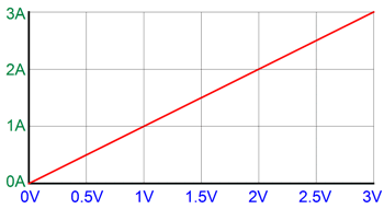
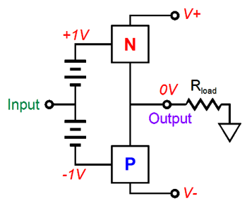
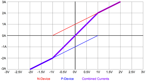
Perfectly constant transconductance, as each 1V increase in input voltage develops an equal 1A increase in current conduction; and no on voltage, as the current flows as soon as the control voltage exceeds zero volts. Now, let's place an N and P version of this perfect device in a class-AB output stage, with a rich 1A idle current.
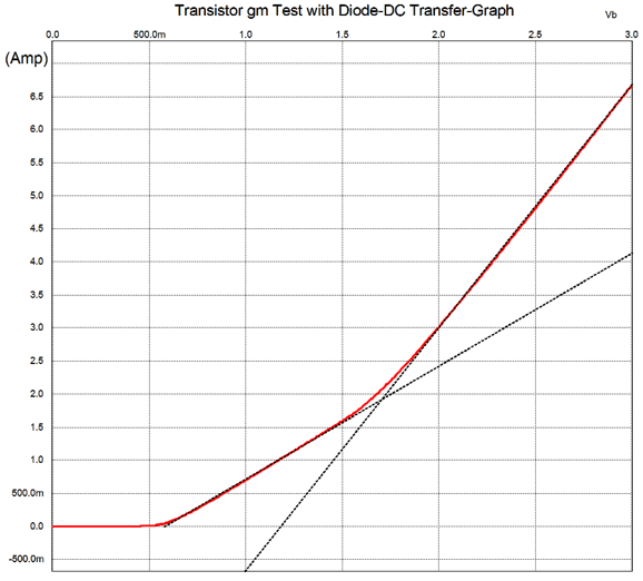
We now measure the effective transconductance of the entire output stage working into a dead short.
Note the tell-tale gm doubling where the two devices overlap in conduction, in spite of perfect output devices being used. (Robert Cordell long ago pointed out that MOSFETs are not perfectly linear devices, as they are slow to turn on, which gives them a lower transconductance before they begin to conduct in earnest, which largely undoes the potential for gm doubling, which, in turn, largely argues for their use in class-AB power amplifiers. I remember reading in an RCA in-house EE journal from the 1950s that sharp-cutoff pentodes and most triodes should be used in class-A push-pull power amplifiers, while gooey-cutoff pentodes and sloppy triodes should be used in class-AB amplifiers, presumably due gm-doubling effects.) Since perfect devices—which do not exist—are not the solution, what is? Two approaches present themselves: we can either pre-treat, i.e. pre-distort the input signal that the gm-doubled output stage sees, so that a doubled gm is prevented, much like eyeglasses pre-distort the image before the eyes see it, creating a sharper focus in the brain. Or, we can create an output stage that corrects the gm doubling afterwards by doubling each output devices' transconductance once the other device cuts off, thereby maintaining a constant-transconductance output stage, with greater linearity and constant output impedance, much like a class-A, push-pull power amplifier does. Either approach would produce the following two-slope graph from our perfect output device.
If we used such a device in a push-pull output stage, we would get altogether different results.
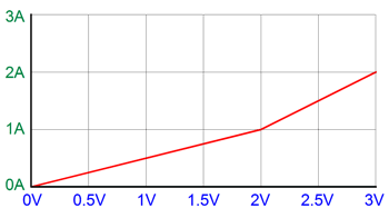
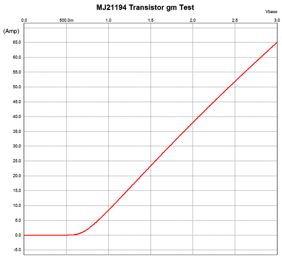
Let's review the transconductance plot for an actual power transistor, the MJ21194 an NPN 250V 16A transistor, before we attempt to deliver a pre-distorted input signal to it. In the following SPICE simulation graph, the bottom axis shows base voltage; the Y axis, collector current. The emitter-to-collector voltage is 30V.
Impressive, both due to its peak current magnitude and linearity, although it shows some slight beta droop at higher currents, which the device's data sheet shows more clearly.
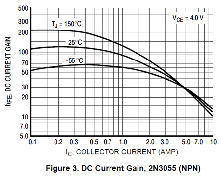
Note how the collector current begins to fall off over 3A. Actually, this transistor is quite impressive. In contrast, the old soldier power transistor that filled many a solid-state power amplifier of decades past, the 2N3055 exhibits a far more droopy current gain, falling off before 500mA is reached.
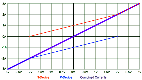
But watch what happens when we create a big fat current overlap (500mA) between MJ21194 NPN & MJ21193 PNP transistors with 0.5-ohm emitter resistors. By the way, 500mA of idle current implies peak current swing of 1A and 4W of class-A output.
Note how over the shared range of conduction, the transconductance doubles; the straight line disappears, replaced by the green lightning-bolt plot. Now, consider what would result if we had used devices that presented two transconductances, two slopes in other words, the first being half that of the second. As long as we carefully chose the idle current, we get the following straight line, which implies a constant gm, as the two half-gm slopes in parallel equal the steeper slope. Since output devices with a sharply bent knee are not sold, we will have to create our own out of preexisting devices. With power transistors, a very simple solution exists: we simply add a base resistor that is shunted by a high-speed diode or rectifier, such as the MUR420G.
Note the added 0.22-ohm emitter resistor, which is a typical value and a necessary component when multiple transistors are used in parallel, as it prevents current hogging. The base resistor's value must be carefully chosen to create two gm slopes that differed by a factor of two. In SPICE simulations, the value turned out to be 16.9 0hms when a 0.22-ohm emitter resistor was used.
The next step is to set the idle current to half of the knee value. For example, if the knee occurs at 1.8A, then we use 900mA as the idle current value, which ensures that the combined transconductance remains constant. Mind you, 900mA is crazy hot even for a 250W transistor, as 0.9A against a 30Vdc power-supply rail voltage equals 27W of heat dissipation at idle from the single transistor. When you do the heatsink math, the 250W rating quickly gets used up. Okay, are done now? No. Although this solution is simple, it does bring its own problems. For example, adding more resistance to the already present base resistance lowers the transistor's transconductance, which is precisely how this trick works; but this also means that we are losing transconductance, not gaining it. Second, the base resistor tends to undo the transistor's linearity. Third, often a small-valued, say 3 ohm, base-stopper resistor is required to prevent transistor oscillations. Well, adding a second base resistor in series will make things even more complicated. And last, transistors present input capacitances which means that the added base resistor will work less effectively at high frequencies. A better place to use the rectifier shunted resistor is before the driver transistor or in front of a MOSFET's gate.
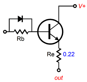
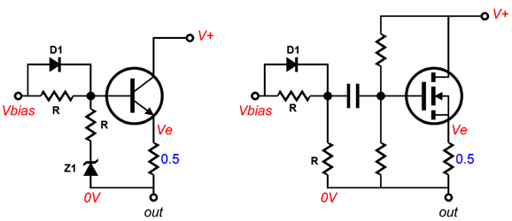
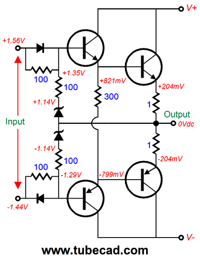
Note how we added an equal-valued second resistor and a zener diode. The two resistors define a two-resistor voltage divider, with a 50% signal reduction up to the point when the rectifier becomes forward biased, which allows 100% of the signal to pass through. This configuration allows the output transistors to retain all of their transconductance and yet allows the output stage as a whole to exhibit a constant transconductance. Much better. The optimal part values are roughly given by the following formulas. Vr = Vd - Ve where Vr is the voltage drop across the resistors; Vd, the diode turn-on voltage; and Ve, the emitter voltage. Thus, Vz, the zener voltage, must equal Vbias - Vr. How do we find Vbias? Vbias is whatever voltage is required to establish the desired Ve voltage.
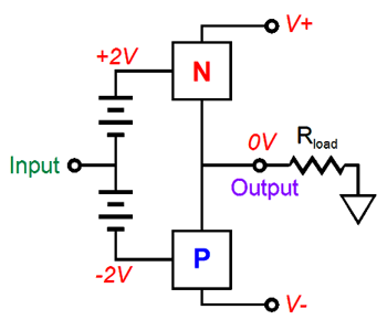
We place the diodes and resistors before the driver stage instead, as the schematic above shows. Here, the output stage's output is fed back to the pre-distortion circuit and the drive transistors deliver the modified signal to the output transistors. Returning to the interesting class-A power buffer circuit that I opened with, could we add the this diode-resistor circuit to it? Yes, but we would select values that only kicked in when a 4-ohm load was encountered and the output stage left its class-A window of operation. To me, this seems too high a price to pay, as we will have halved the output stage's gm even when driving 8-ohm loads and when still comfortably within the class-A window. Next time, I will present a better solution for the class-A power buffer.
Next Time
*Rich Class-AB
User Guides for GlassWare Software Since I am still getting e-mail asking how to buy these GlassWare software programs:
For those of you who still have old computers running Windows XP (32-bit) or any other Windows 32-bit OS, I have setup the download availability of my old old standards: Tube CAD, SE Amp CAD, and Audio Gadgets. The downloads are at the GlassWare-Yahoo store and the price is only $9.95 for each program. http://glass-ware.stores.yahoo.net/adsoffromgla.html So many have asked that I had to do it. WARNING: THESE THREE PROGRAMS WILL NOT RUN UNDER VISTA 64-Bit or WINDOWS 7 & 8 or any other 64-bit OS. One day, I do plan on remaking all of these programs into 64-bit versions, but it will be a huge ordeal, as programming requires vast chunks of noise-free time, something very rare with children running about. Ideally, I would love to come out with versions that run on iPads and Android-OS tablets.
//JRB |
Kit User Guide PDFs
And
High-quality, double-sided, extra thick, 2-oz traces, plated-through holes, dual sets of resistor pads and pads for two coupling capacitors. Stereo and mono, octal and 9-pin printed circuit boards available.
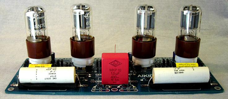
Designed by John Broskie & Made in USA Aikido PCBs for as little as $24 http://glass-ware.stores.yahoo.net/
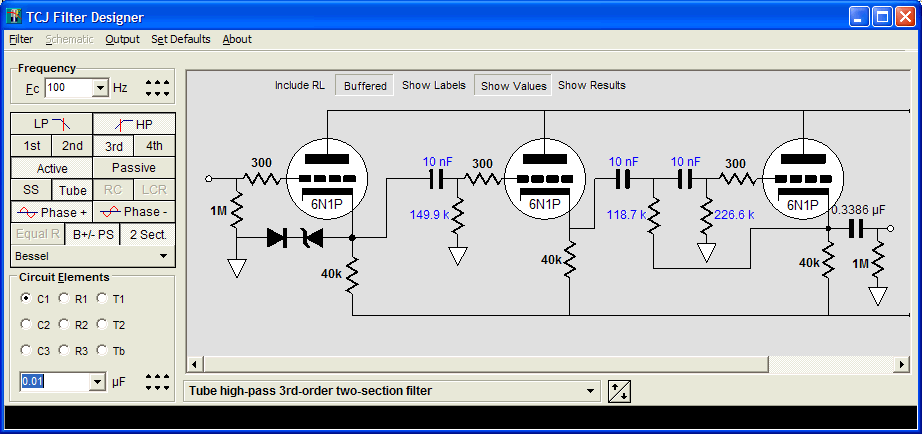
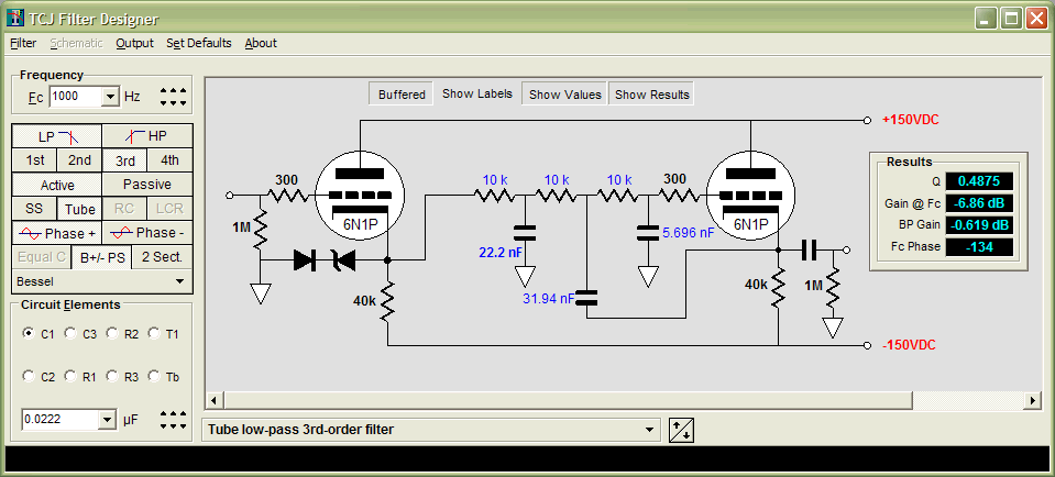
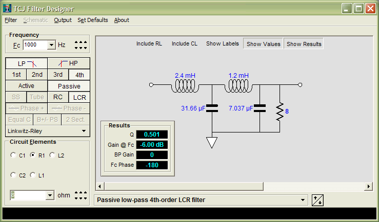
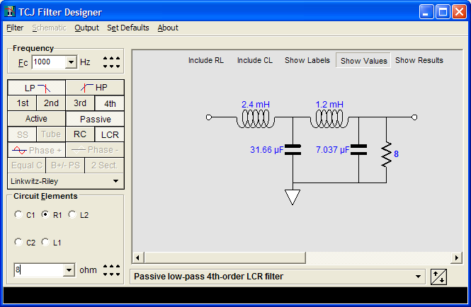
The Tube CAD Journal's first companion program, TCJ Filter Design lets you design a filter or crossover (passive, OpAmp or tube) without having to check out thick textbooks from the library and without having to breakout the scientific calculator. This program's goal is to provide a quick and easy display not only of the frequency response, but also of the resistor and capacitor values for a passive and active filters and crossovers. TCJ Filter Design is easy to use, but not lightweight, holding over 60 different filter topologies and up to four filter alignments: While the program's main concern is active filters, solid-state and tube, it also does passive filters. In fact, it can be used to calculate passive crossovers for use with speakers by entering 8 ohms as the terminating resistance. Click on the image below to see the full screen capture.
Tube crossovers are a major part of this program; both buffered and un-buffered tube based filters along with mono-polar and bipolar power supply topologies are covered. Available on a CD-ROM and a downloadable version (4 Megabytes). |
||


| www.tubecad.com Copyright © 1999-2015 GlassWare All Rights Reserved |