| John Broskie's Guide to Tube Circuit Analysis & Design |
14 May 2016 Post 379
Upside-Down Differential Amplifier
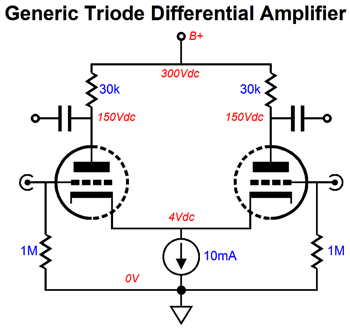
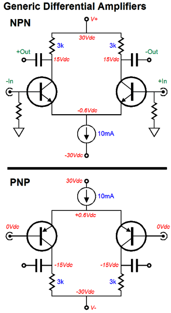
No negative power-supply rail voltage is needed, as the two cathodes sit 4-volts above ground level. With NPN transistors or N-channel MOSFETs, however, a negative power-supply rail voltage is needed. With PNP transistors, a positive power-supply rail voltage is needed.
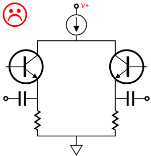
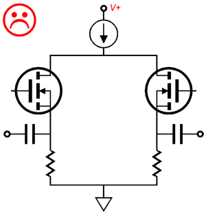
So far, everyone is on the same page. Now, let's throw in something new. What happens if we turn the constant-current source and load resistors upside-down?
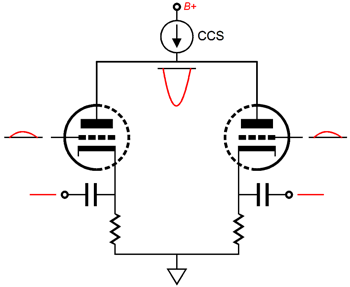
The sad face says it all. This topology won't work, nor will the following.
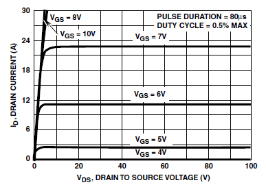
Why not? The transistor's collector and the MOSFET's drain are supremely indifferent to the voltage imposed upon them. Here is a MOSFET's drain curves.
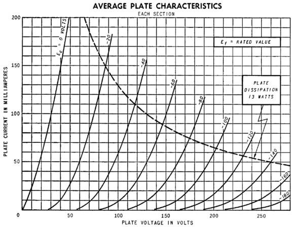
Note how, as we slide up the drain voltage on the 6V gate line, say from 10V to 100V, the current conduction remains dead constant. Triodes are different, as the triode's plate is sensitive to plate voltage. How much so? The triode's plate is 1/mu (amplification factor) as sensitive as its grid. For example, a 6AS7 has a mu of 2, so its plate is half as effective in controlling current flow through the triode as is its grid. Follow the -20V grid in the following graph from 60V to 80V and you see the current conduction go from 50mA to 120mA. (Divide the 20V by the 0.07A delta and you get the plate resistance, i.e. 286 ohms.)
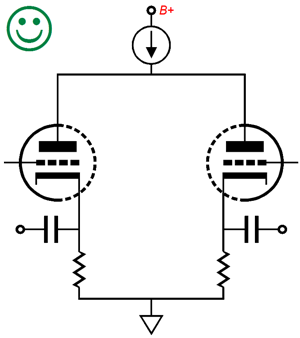
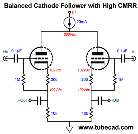
Because the triode's plate is sensitive to plate voltage, the following topology will work, with the two grids seeing a balanced pair of input signals.
This allows us to create a balanced cathode follower with excellent common-mode rejection ratio (CMRR). In balanced circuits, CMRR is an important specification, as noise is usually a common-mode signal, which a high CMRR can greatly attenuate.
If the same signal is presented to both grids, the cathodes remain locked at their idle voltage. In other words, this balanced cathode follower will not respond to signals that are common to both inputs.
For example, if both grids of a 6AS7 see a 10Vpk positive pulse, then the only way the two triodes can each maintain half the CCS current is for the plates to see a peak negative pulse of -20V, as the 6AS7's mu of 2 sets the ratio of +1 to -2. Conversely, if the grids saw a -10V pulse, the plates would have to climb +20V in voltage to maintain the same constant-current flow from the two triodes. The secret to the triode working in this upside-down differential topology is its plate resistance. Pentodes, FETs, MOSFETs, and transistors, in contrast, present at their plates, drains, and collectors resistances that can approach infinity. (If you come from the tube world, the constant-current source might be mentally tripping you up here; imagine it replaced by a large-valued inductor. Conversely, if you come form the solid-state world and inductors trip you up, then imagine them replaced with constant-current sources.) If this topology looks a bit familiar, it is probably due to you having seen it seven years ago in post 191, where I referred to it as a plate driven phase splitter.
And this hybrid power amplifier is worthy of close examination. (As I look at it now, seven years later, I would lose the 30µF capacitor and add two coupling capacitors, one for each MOSFET. In addition, I would replace the 28k plate resistor with a constant-current source, which would allow us to drop the 300V B+ voltage down to 240Vdc. All in all, a truly interesting circuit, even if I do say so myself. What if we reduced the 60V B+ voltage down to 30Vdc adn ran the output MOSFETs in class-A....)
I recommend that you read this post, as shows several interesting variations and offers a good overview of the plate-driven topology. Since I mentioned phase splitters, let's turn the balanced cathode follower into a phase splitter.
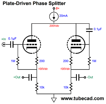
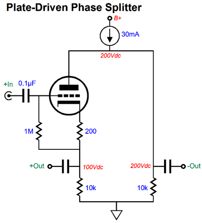
Did your head explode? Sorry, I probably made too big a leap. Let us try again with baby steps. We start by placing a split-load phase splitter's two load resistors horizontally, rather than the usual vertical arrangement. The triode will draw 10mA, while the 10k resistor on the right will draw 20mA, as 200V/10k equals 20mA.
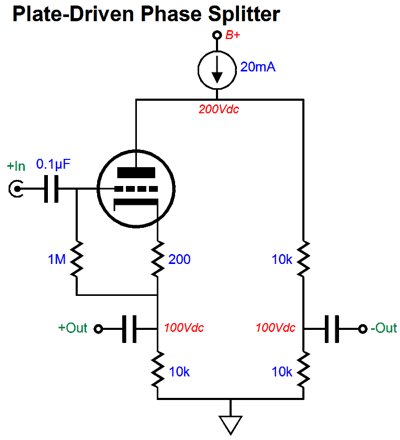
The CCS presents an astronomically high impedance, so it effectively falls out of the AC equations. Any current-flow change that the left 10k cathode resistor experiences, the right plate resistor must also experiences, albeit in an inverted way. As one goes up, the other goes down. As one goes down, the other goes up. At idle, both resistors experience the same 10mA of current flow. If the left 10k cathode resistor experiences an increase of current flow of 1mA, then the right 10k cathode resistor experiences a decrease of current flow by 1mA. The result is two out-of-phase output signals. We can save on current flow by using two 10k resistors in series.
Now the CCS can be set to 20mA, rather than the previous 30mA. The triode's plate must, however, undergo twice as large voltages as in the previous example, so this variation might require a higher B+ voltage. Now that we have the basics down pat, I can move on to the circuits that I actually wanted to start with, but which I knew would cause to many headaches if shown without preparation.
Graham Maynard's GEM Amplifier
This reminds me of what Lynn Olson has been saying for a long time now: loudspeakers are not resistors; they are, instead, wily, crazy reactive loads, which can back-feed into the amplifier, causing sonic distress. Well, Mr. Maynard created his own solid-state power amplifier, the GEM, that combined a single-ended, class-A output stage with class-AB output stage. In addition, his GEM design used an interesting nested feedback loop within the driver and output stages. Here is a link to the schematic. Trust me, it is not as complex as it looks. Here is the general overview of the GEM amplifier.
Maynard describes his effort thus:
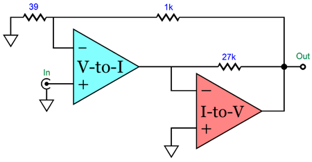
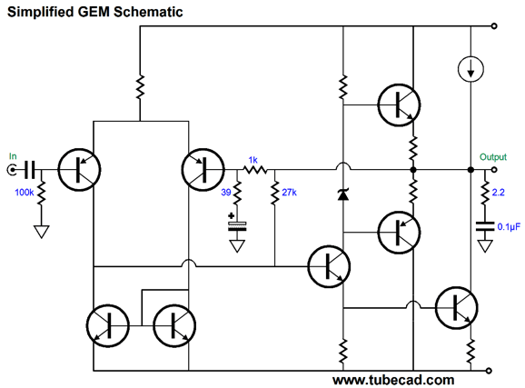
I bet that you didn't know that is what "KT" stands for in such tubes as the KT66, KT77, and KT88. Here is a simplified version of his GEM Schematic:
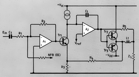
The AC input signal enters a differential amplifier made up of the two PNP transistors, whose collectors terminate into a current mirror, and which feed an NPN common-emitter amplifier, whose emitter drives the bottommost, rightmost NPN transistor, which runs in class-A, as it is loaded by the constant-current source. The NPN common-emitter amplifier's collector also drives the class-AB output stage. No output inductor is used. The 27k negative-feedback resistor provides 20dB of nest negative feedback. I am reminded of the Quad current-dumping amplifier which used a small class-A in parallel with a big class-B amplifier, as shown below.
Maynard's design differs in that the driver stage drives both the class-A and class-AB output stage; in contrast, the Quad design has the class-A amplifier driving the class-B output stage. In addition, the Maynard design uses two feedback loops, while the Quad uses three. Okay, now let's add a tad bit more to the GEM's simplified schematic.
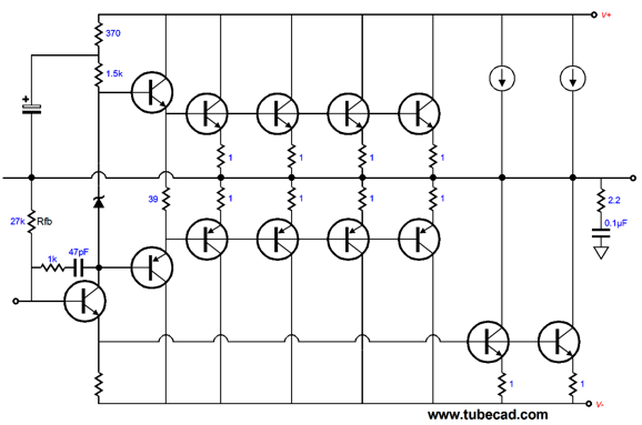
The input stage differential amplifier's long tail gets an RC filter and the driver stage gets a bootstrap capacitor. The other side of the current mirror gets a its own 27k load resistor to ground and an extra nested high-frequency feedback loop is provided by the 1k resistor and 47pF capacitor. The actual GEM output stage holds 12 power transistors.
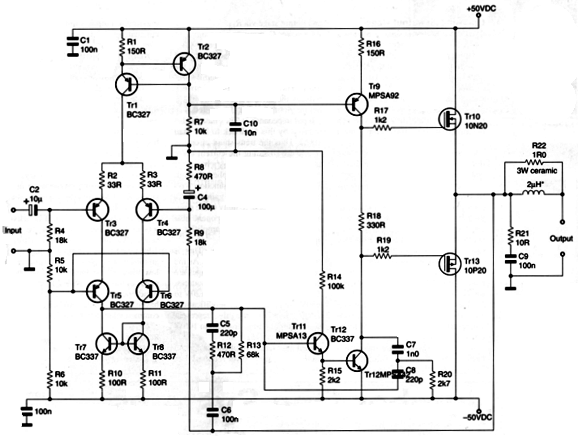
The two constant-current sources are each made up of a PNP transistor and emitter resistor. Maynard's use of the 27k feedback resistor is interesting and it reminds of what Russell Breden designed in the June 2000 issue of Electronics world, in an article titled, "A New 100W Class-B Topology."
Breden uses a 68k Rfb resistor (R13)) and a Darlington driver stage to increase the input impedance of the stage. (The grabbled portion of the schematic near Tr12 appeared in the original schematic, [SIC] in other words.) If you have access to the magazine, I recommend that you read his article, as it is full of amplifier-design insights. Okay, what to make of these two designs? In general, I quite like nested negative feedback loops, but both Brenden's and Maynard's designs suffer from a flaw, the sort of flaw you won't see in SPICE simulations—unless, of course, you go hunting for it. The global negative feedback terminates into ground. We assume that ground, by definition alone if nothing else, is noise-free. The same, however, cannot be said of the positive and negative power-supply rails. These babies are chock full of ripple and rectifier hash. In addition, their voltages sag under heavy use. The +/-50V rails at idle can fall to +/-40V under heavy loading. Is this a problem? Let's return to the generic solid-state power amplifier to see what can go wrong.
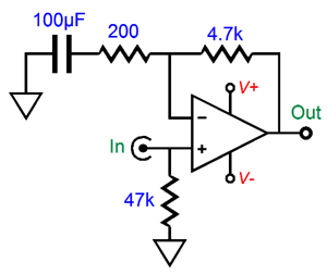
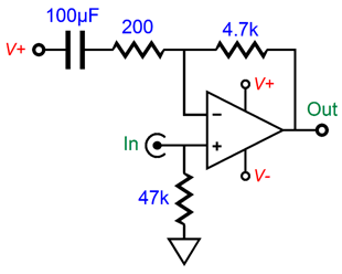
The 200-ohm feedback resistor AC "grounds" into ground through the 100µF capacitor. Great. What if we terminate the 100µF capacitor to the positive power-supply rail instead?
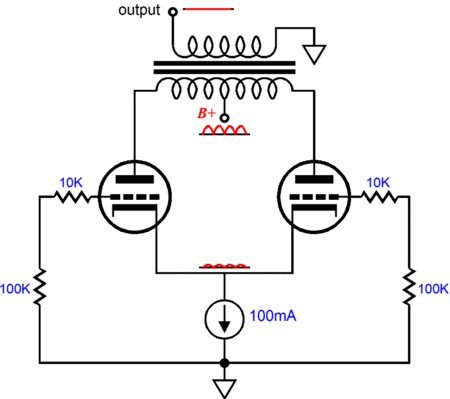
Not so great, which may not appear not great so at first, as no DC offset occurs at the output, for the capacitor ensures 100% DC feedback. Moreover, in SPICE simulations, no difference can be discerned between this alternative circuit and the regular "grounded" version. Reality, on the other hand, will kick you in the pants, good and hard. Real power-supply rails are nasty things, filled with nasty ripple and nasty rectifier noise, harsh harmonics and possible ringing. The above amplifier will amplify this nastiness by 23.5 times, so 100mV of ripple will become 2.35v of ripple at the output. Had we terminated the 100µF capacitor to the negative power-supply rail instead the same results would occur. If thing that negative feedback will save the day, you are wrong. The negative feedback mechanism compares the output to positive rail and ensures that the power-supply noise is amplified as a signal, which it is in this configuration. Now, look back at Brenden's and Maynard's designs. Both assume that the negative power-supply rail won't prove to be an electric sewer—or hope that the global negative feedback loop will save the day by undoing what the sewer has wrought. This last hope is fairly sound, but notice that we have just needlessly burdened the negative feedback with extraneous noise to eliminate. Perhaps, Brenden's design will offer fairly clean output at idle, as his class-B operation of the output devices means that little idle current flows. In contrast, Maynard's design draws a considerable amount of current at idle, due to its semi-class-A operation, so we would expect its power-supply rails to prove dirtier. But Brenden's design isn't off the hook, as once the music plays, the power-supply rails will get banged about by the big demands made by the output stage. I call this sort of problem dynamically-induced poor PSRR. Surely, you have heard amplifiers that sound clean at low levels, but then take on a hazy, grimy quality at higher volume. Even tube amplifiers are guilty. In the classic push-pull tube power amplifier, the two output tubes both draw current at idle, so the amplifier measures quiet at idle. (Imagine the constant-current source being shunted by a large-valued capacitor.)
Now, remove one output tube and measure the PSRR. The PSRR got much worse. Why? The output transformer no longer sees an equal amount of ripple at both its ends; instead, it sees 100% of the ripple at its center tap and say 33% of the ripple at the single output triode's plate. Remember, where there is a difference, there's an output signal from the output transformer. The same dynamically-induced poor PSRR occurs in OTL amplifier that use bipolar power supplies and in Circlotron amplifiers that use triodes as output devices. Pentodes, MOSFETs, and transistors side step dynamically-induced poor PSRR to large degree due to their high plate, drain, and collector impedances, which make poor AC voltage dividers; their input and driver stages, however, may not escape the signal-induced power-supply noise. No doubt you have seen the following power-amplifier power-supply design.
The idea here is to isolate each channel's amplifier from the other channel's amplifier. If the right channel gets slammed by a massive drum roll, the left channels amplifier does not suffer the same rail voltage collapse that the right channel suffers. True, we loose the voltage dropped across the added rectifiers, but an MUR420G super-fast rectifier only drops about 0.5V at idle currents and 0.7V at the most heavy current flow. Moreover, the higher the rail voltage, the less the rectifier drop matters. Returning to Brenden's and Maynard's designs, the easy fix is to use a mono-polar power supply. Both designs are already capacitor coupled at their inputs, so all that would be needed is a large-valued coupling capacitor at the output. (Before anyone is tempted to say ick, remember that the famous Futterman OTL amplifiers were capacitor coupled as are many excellent power amplifiers.) Both the nested and global feedback loops will now be ground referenced.
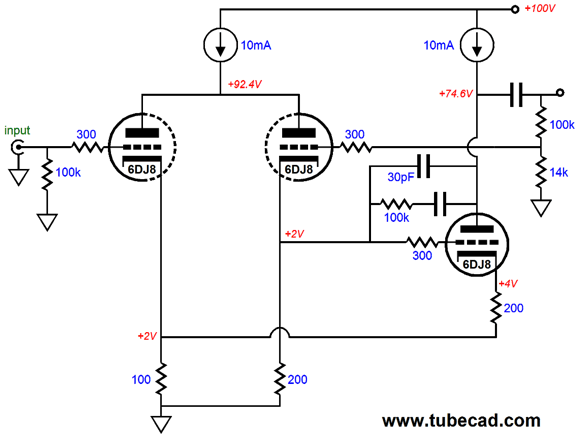
Upside-Down Differential Amplifier in Use
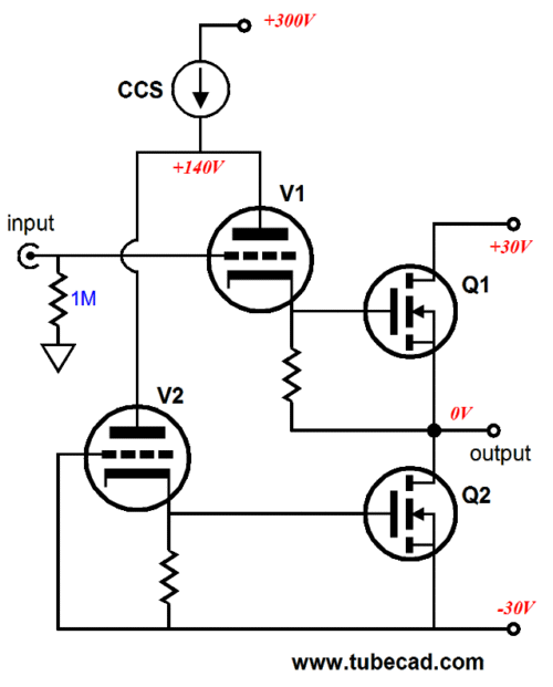
As configured, this is only a line-stage amplifier. Of course, we could replace the 6DJ8 output tube with a 6AS7 or triode-connected pentode and use the amplifier as a headphone amplifier. Note how the output triode is being driven in a push-pull fashion, as it receives input signals at both its grid and cathode. Another variation is the following.
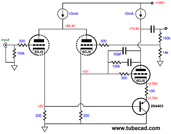
The PNP transistor drives the output triode's cathode. Another possibility is to go full hybrid.
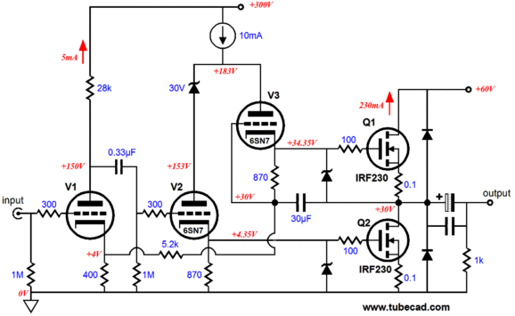
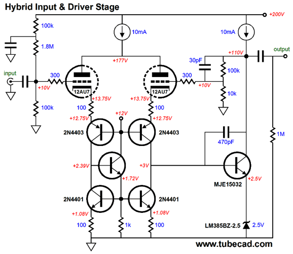
The plate-driven input stage is cascoded by the 2N4403 PNP transistors. The 2n4401 NPN transistors define a current mirror. The MJE15032 NPN transistor functions as a common-emitter amplifier. Note how the DC offset of 10Vdc becomes a DC offset of 110Vdc at the output before the coupling capacitor. Where's the nested feedback resistor? In SPICE simulations, I found that it didn't improve the performance. But then, I used a purely resistive load in simulations. Perhaps, Maynard is right about its need in a power amplifier driving complex inductive loads, such as your speakers. Here is one last possible topology: a hybrid power amplifier that makes use of the plate-driven phase splitter.
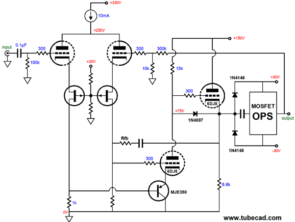
I was assuming that a 6SN7 would be used as the input tube. If a higher transconductance tube were used, such as the 6DJ8 or ECC99 or 5687, the following design could be run under lower power-supply rail voltages.
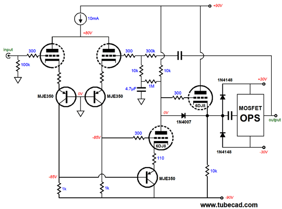
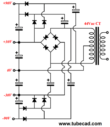
We must lose the nested feedback resistor, due to the bipolar power supply and its noisy negative rail. The 1M resistor allows the input stage to center the driver stage's output voltage, as the output is AC coupled to the negative feedback loop, while the driver stage's output is DC coupled, but not AC coupled. (The coupling capacitor in series with the 300k resistor need only be 0.1µF in value.) The two 1N4148 diodes prevent the MOSFET, unity-gain output stage from being damaged by the driver stage. (A DC servo loop could be used to eliminate the DC offset at the amplifier's output.) The power supply only requires a 44Vac-CT secondary to create the +/-30V and +/-90V rail voltages. The heater elements will require their own power supply(s).
It's happened again: what I thought would be a short missive, dispatch has turned into a 2,800-word long tome. I have to stop now, before my fingers fall off.
//JRB
Special Thanks If you have been reading my posts, you know that my lifetime goal is reaching post number one thousand. I have 621 more to go. I should easily be able to hit post 400 this year. My second goal is to gather 1,000 patrons. I have 965 patrons to go. If you enjoyed reading this post from me for the last 18 years, then you might consider becoming one of my patrons at Patreon.com.
//JRB
User Guides for GlassWare Software Since I am still getting e-mail asking how to buy these GlassWare software programs:
For those of you who still have old computers running Windows XP (32-bit) or any other Windows 32-bit OS, I have setup the download availability of my old old standards: Tube CAD, SE Amp CAD, and Audio Gadgets. The downloads are at the GlassWare-Yahoo store and the price is only $9.95 for each program. http://glass-ware.stores.yahoo.net/adsoffromgla.html So many have asked that I had to do it. WARNING: THESE THREE PROGRAMS WILL NOT RUN UNDER VISTA 64-Bit or WINDOWS 7 & 8 or any other 64-bit OS. One day, I do plan on remaking all of these programs into 64-bit versions, but it will be a huge ordeal, as programming requires vast chunks of noise-free time, something very rare with children running about. Ideally, I would love to come out with versions that run on iPads and Android-OS tablets.
//JRB |
Kit User Guide PDFs
And
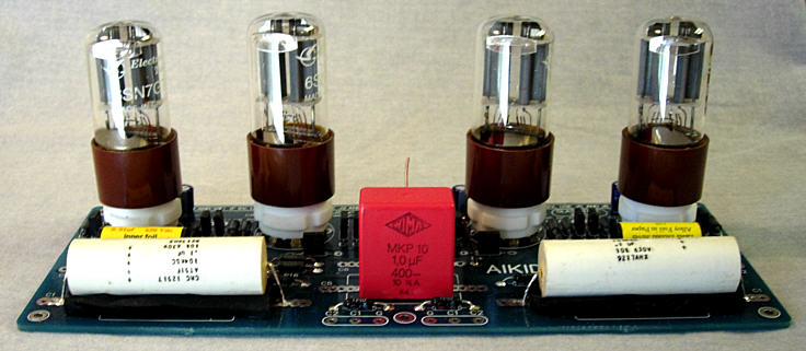
High-quality, double-sided, extra thick, 2-oz traces, plated-through holes, dual sets of resistor pads and pads for two coupling capacitors. Stereo and mono, octal and 9-pin printed circuit boards available.
Designed by John Broskie & Made in USA Aikido PCBs for as little as $24 http://glass-ware.stores.yahoo.net/
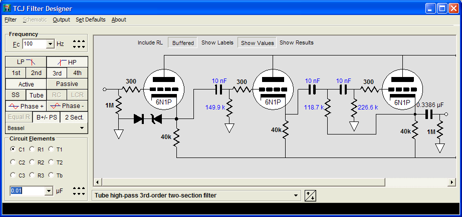
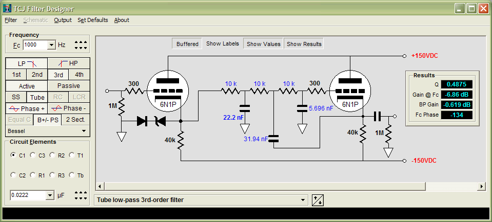
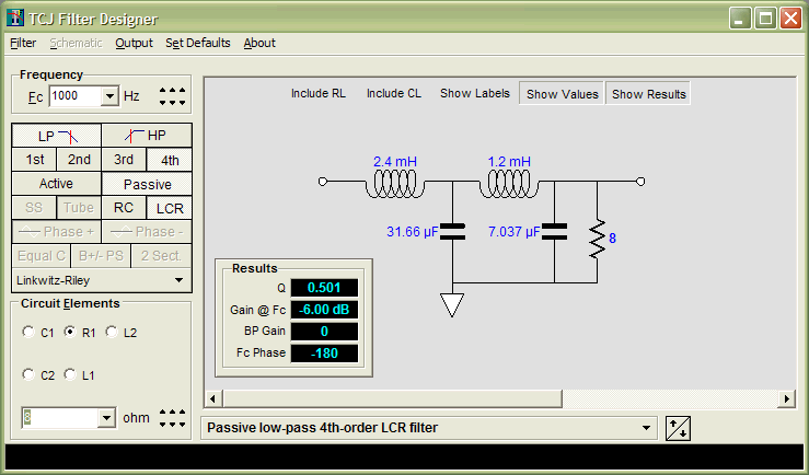
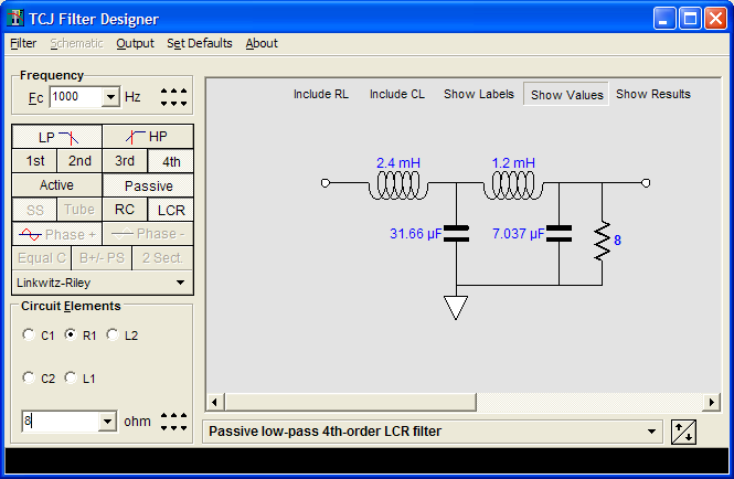
The Tube CAD Journal's first companion program, TCJ Filter Design lets you design a filter or crossover (passive, OpAmp or tube) without having to check out thick textbooks from the library and without having to breakout the scientific calculator. This program's goal is to provide a quick and easy display not only of the frequency response, but also of the resistor and capacitor values for a passive and active filters and crossovers. TCJ Filter Design is easy to use, but not lightweight, holding over 60 different filter topologies and up to four filter alignments: While the program's main concern is active filters, solid-state and tube, it also does passive filters. In fact, it can be used to calculate passive crossovers for use with speakers by entering 8 ohms as the terminating resistance. Click on the image below to see the full screen capture.
Tube crossovers are a major part of this program; both buffered and un-buffered tube based filters along with mono-polar and bipolar power supply topologies are covered. Available on a CD-ROM and a downloadable version (4 Megabytes). |
||


| www.tubecad.com Copyright © 1999-2017 GlassWare All Rights Reserved |