| John Broskie's Guide to Tube Circuit Analysis & Design |
15 November 2009
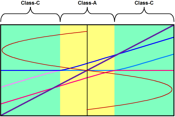
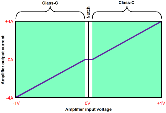
Class-AC Gm doubling? What is gm doubling? While most know about crossover-notch distortion in push-pull power amplifier, few have heard about gm doubling in push-pull amplifiers. When running a push-pull output stage in anything less than class-A mode, be it in a tube-based amplifier or a solid-state amplifier, the issue of device overlap must be addressed. If the two devices do not overlap in their current conduction, a notch in the transfer curve will occur, wherein no output signal is forthcoming.
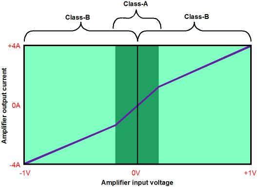
The usual solution is to run the output stage in class-AB, with both devices working in tandem over a small overlap range of current conduction. Depending on the devices used, getting the right amount of overlap can be difficult. For example, with transistors, the base-to-emitter voltage is not constant, as it varies with heat. So, the right amount of current at idle may no longer be correct for a hot output stage. Well, why not just make the overlap wider? The problem with running a rich class-AB lies in gm doubling, wherein the output stage’s effective transconductance doubles in the class-A range of operation, where both devices work in unison in response to the input signal. Because of the doubled transconductance in the class-A overlap range, the output impedance is also effectively halved (and the linearity greatly improved). But once one output device turns off, the output stage is back in class-B mode, with half the transconductance and twice the output impedance (and often with a much worse PSRR figure). This is the problem of gm doubling.
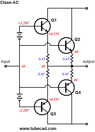
Of course, lots of negative feedback will hide much of the distortion that arises due to the discontinuity in conduction between output devices. Furthermore, the load itself provides a powerful antidote, as the load resistance greatly limits the effective transconductance of the output stage. For example, with a load resistance of 10 ohms, the maximum effective transconductance of an output stage can never be more than 100mA per volt. Still, the underlining discontinuity remains, although greatly subdued by the load resistance. And most solid-state power amplifiers enjoy huge amounts of open-loop gain with which to drive their negative feedback loops. But what if one decides to eschew high negative feedback, in spite of its promises of low distortion and output impedance? (Much as a sturdy individual might turn his back on socialism’s siren song, in spite of the advertised free food, free health care, free housing...) Without gobs of negative feedback, gm doubling and crossover-notch distortion are taller hurdles to jump. Besides, an output stage that operated free of gm doubling and crossover-notch distortion would benefit even more from application of negative feedback, as it would produce less that needed fixing. Class-AC operation requires at least two pairs of output devices per channel, for a total of four devices. The primary set of devices runs under a high idle current that ensures a wide range of class-A output, say 4W to 16W. The secondary set is completely turned off at idle and only conducts when the primary set falls out of class-A mode. In other words, in the class-AC output stage, gm doubling is corrected by making it a constant, as two of the four output devices are always on over the entire range of output swing, so twice the gm of any single output device is always provided. Let’s start with a solid-state example, as it shows the differing phases of conduction between output devices more readily than a tube-based example. (If you do not speak solid-state, then feel free to skip to the tube-based class-AC examples.)
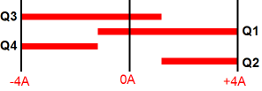
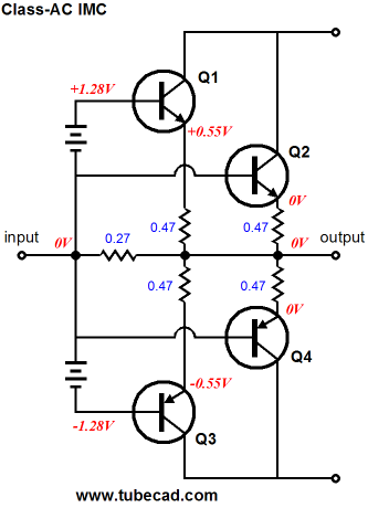
Transistors Q2 and Q4 draw no current at idle, as their bases are attached the same voltage as their emitters. Only when the input signal swings high enough to reach their threshold voltage, do they conduct. In other words, at background-music levels, these two output devices may never conduct and the power amplifier will operate in pure class-A mode entirely, as transistors Q1 and Q3 never cease to conduct. But once the input signal is increased beyond the bounds of class-A operation, the secondary transistors, Q2 and Q4 enter the battle. As Q1 turns off, Q4 kicks in; as Q3 turns off, Q2 fires up.
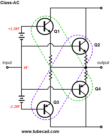
One way to look at the Class-AC configuration is to view transistors Q1 and Q4 as being paired push-pull partners and Q2 and Q3 as also pairing up. In other words, transistors Q1 and Q4 define a class-B (AB) pair while Q2 and Q3 define a matching class-B pair.
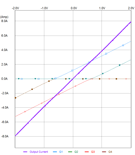
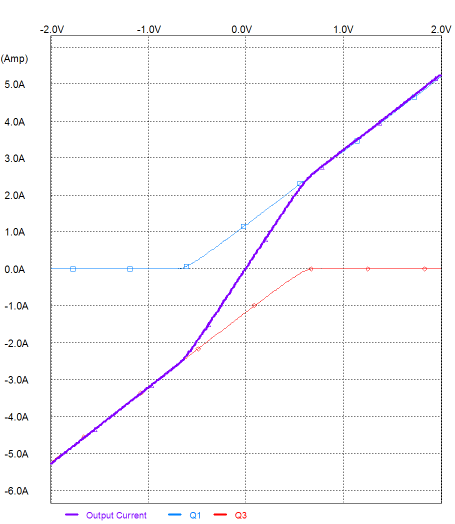
So how well does this setup work? We will start with the severest of loads: 0 ohms, a dead short to ground. What follows is a SPICE simulation graph. The transistors used are MJ15022 (NPN) and MJ15023 (PNP) types.
As can be gleaned from the above graph, the linearity is first-rate. The purple line traces the current delivered into ground by the output stage. The blue, green, red, and brown lines trace the four transistors current contribution against the sweep from -2V to +2V at the output stage’s input. This is as bad as it gets, as the addition of any load resistance will further linearize the transfer curve! Now let’s take a look at what is the contribution made by just the primary transistors, Q1 and Q3. In other words, in the following graph we see the transfer curve of a richly biased class-AB output stage.
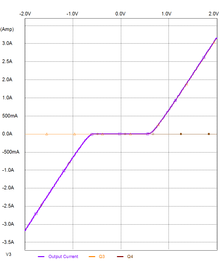
There is the dreaded gm doubling effect laid bare. Where the two output devices conduct in unison, the effective transconductance is doubled, resulting in the steep portion at the center of the curve; but once one device cuts off, the curve’s slope droops to half its overlapped value. In the following graph, we see the contribution of the secondary transistors, Q2 & Q4. From about -0.7V to +0.7 of base-voltage swing, the pair of transistors do nothing; they sit idle, drawing no current. Once the transistors’ threshold is reached, the transistors turn on and contribute to the task of driving the load. (By the way, the following graph also illustrates a severe case of crossover-notch distortion.)
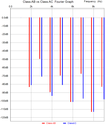
Combining the last two graphs creates the first graph, with its super straight transfer plot. Nirvana? Well, to be honest, my solution is a clever remedy for an illness that few get. What? The problem of gm doubling, for the most part, doesn’t really exist. Yes, I am overstating my standpoint for emphasis. The problem of gm doubling is real, but it finds an easy and fairly effective antidote in the external load resistance. The load saves the day. The load resistance acts like an unbypassed cathode (or emitter or source) resistor, which linearizes the output device by giving up transconductance. For example, what happens with two output transistors configured as a push-pull emitter pair—the output stage that is used in 99.9% of solid-state power amplifier—over their overlap region? The load resistance is effectively seen as doubled by the two transistors, so 8 ohms becomes 16 ohms. Thus, with two transistors are working together, thereby doubling the transconductance of a single transistor, each transistor effectively holds a 16-ohm emitter resistor over the amplifier’s range of class-A operation. But once one output device turns off, the amplifier leaves class-A mode and moves into class-B, with the lone active transistor now seeing an 8-ohm emitter resistor. In other words, the load resistance self-corrects the ills of gm doubling. Well, once again I have overstated, but not by much. The lower the load resistance, the bigger the gm doubling predicament becomes; conversely, the higher the load resistance, the smaller the problem. So, we have continuum of self-correction. In other words, gm doubling limits an amplifier’s goal of perfect amplification, but not by as much as we might conclude from a quick theoretical analysis. Having said all this, I actually do believe that I can hear the malicious effects of gm doubling and I am sure that I am not alone. Have you heard the same thing that I hear when an otherwise good sounding solid-state power amplifier is burdened by a 4-ohm (or lower) load, even when the amplifier is not overly tasked? (I once built a low-voltage power amplifier to drive my 0.5-ohm Strathern ribbon loudspeakers. The speakers came with a step-down toroidal transformer, but I was convinced that the transformer added more sonic blemishes than I could live with. The transformer held a winding ratio of about 4:1, which implied an impedance ratio of 16:1. Thus, I concluded that if I took a quality solid-state power amplifier and scaled the rail voltages down by four, I would get all the output voltage swing the drivers needed. In other words, instead of using +/-40V power supply rails, my amplifier would use +/-10V rails—the actual rail voltages I used were closer to 12V, with a set of secondary rails at +/-24V for the input and VAS stages. How did it sound? Just dreadful. Amazingly harsh. Yet, the amplifier had sounded quite good with 40V rails or when driving 8-ohm loads. I scratched my head a great deal and performed a few experiments. The best solution was to up the output stage idle current from 100mA to something close to 1A! I didn’t try 1.6A, but it might have proved the optimal amount of idle current, as 8/0.5 = 16. By the way, cable termination was critical; all contacts had to be crazy tight and the loudspeaker cable had to be super-low in resistance. As I tightened the binding posts with a socket wrench, I could hear the sound level increase!) So, when driving an 8-ohms, how much better is my class-AC configuration over a traditional, although super richly biased, class-AB output stage (16W class-A)? The following graph shows the results from a SPICE simulation of both output stage configurations with 30Vpk voltage swings into an 8-ohm load. (At low signal levels, both amplifiers function identically, as only one pair of transistors is employed in both amplifiers.)
So, which won? The lowest 2nd harmonic winner, by just a smidgen, is the class-AB output stage, but with the 3rd, 4th, 5th, 7th, 9th harmonics, the clear winner is the class-AC output stage by an over -20dB greater reduction on the 3rd and 7th harmonics; and the 6th and 8th harmonic race ended in a tie. By the way, this simulation was of just the output stages and a large overlay of negative feedback would further decrease the distortion harmonics in an actual amplifier. In reality, the class-AC output stage performs much better than the actual very-lean class-AB output stage that 99.5% of solid-state power amplifiers run. For example, nobody uses 0.47-ohm emitter resistors, as they are too large in size, too expensive, and drop too much precious voltage at peak current swings. Remember few amplifier manufacturers would be willing to lose 5W out of the potential 100W the same power amplifier would produce with 0.1-ohm emitter resistors. Moreover, the typical 100W solid-state amplifier would not measure markedly worse than the same amplifier outfitted with the class-AC output stage—at full output that is. But if 95% resides in the first watt, shouldn’t we be checking out the distortion at 1W or 100mW, rather than at 100W? Most solid-state amplifiers would prefer that you didn’t, as most of them produce their lowest distortion figures not at 100mW or 1W, but at 4W to 10W. In contrast, most tube power amplifiers, particularly single-ended tube amplifiers, display their lowest distortion at 100mW (if the amplifier isn’t too noisy) and their distortion slowly climbs with output. In a nutshell, this probably explains why tube amplifiers sound so much more natural than their solid-state brothers.
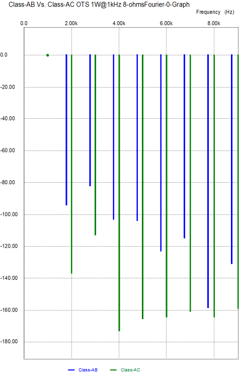
So, if we compare the class-AC output stage with 0.47-ohm emitter resistors to a typical lean-running, class-AB output stage with 0.1-ohm emitter resistors and an idle current of 100mA (most run closer to 50mA), we see a marked difference in distortion at 1W into 8 ohms, as the graph above makes clear.
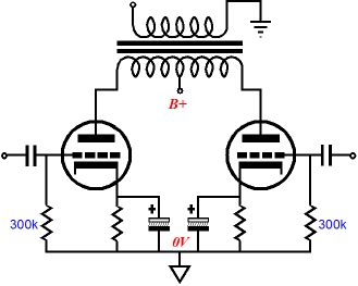
Class-AC & Tubes In fact, since so few tube power amplifiers run a cathode-follower-configured output stage, my class-AC strategy might prove more valuable to the tube amplifier designer. Remember how the load resistance effectively acts as an unbypassed cathode (or source or emitter) resistor. (When the output tubes in a tube push-pull power amplifier are grounded, the load resistance loads the plate, not the cathode. True, a triode-based amplifier will indeed benefit in linearity because of the plate load, but a pentode is much less influenced by the load resistance.)
So, how do we create a class-AC tube-based output stage? One danger we immediately face is that the tubes, unlike transistors, do not like being turned off for prolonged periods of time.
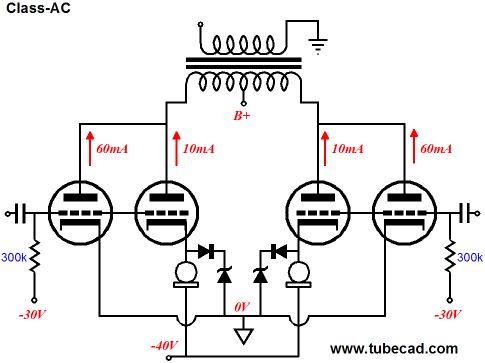
Back in the days of tube-based computers, researchers discovered that the tubes were suffering from sleeping disease, cathode-interface resistance due to their being held in hot but off states for much of their operational life. In other words, most tubes must experience a current flow from cathode to plate to ward off sleeping disease. This is a big problem for a class-AC tube output stage, as the whole point is to keep one pair of tubes off for 90% of the time the amplifier is used, musical peaks being few and briefwell, at least with quality music ;) . The workaround might be to do something along the following lines.
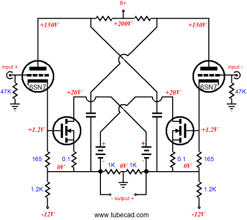
The idea here is that the outer pair of output tubes is primary and the inner pair, secondary. When the primary pair move out of class-A mode, the secondary pair fire up. So far, this functioning is similar to the solid-state design example already covered. The tube example differs in that the inner pair of tubes never cut off. Yes, yes, yes, I know that this is a dangerous bit of knowledge in the hands of a marketing department. Can you not see the big ads proudly proclaiming pure class-A —on the cheap no less. Yes, the secondary pair of tubes never ceases to conduct, as the constant-current source at those tubes' cathodes moves their cathode voltages down to the voltage required to maintain the 10mA idle current, no matter how negative the input signal swings negative (within reason, of course, as the -40V negative power supply rail voltage sets a limit to the constant-current source potential negative swing). But these inner tubes provide no amplification or output impedance as long as the zeners are not activated, as constant current means constant current. But once the input signal swings positively enough to engage the zener trip voltage, the secondary tubes’ cathodes lock in place as if they were ground, albeit at a higher DC voltage, and the tubes contribute to the power amplifier’s output. By the way, I described a similar trick ten years ago here in the Tube CAD Journal:
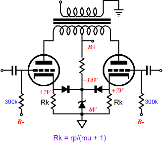
Ten years ago! Is that possible? The mind reels. Here’s an interesting question: How do we achieve class-AC with just two output tubes?
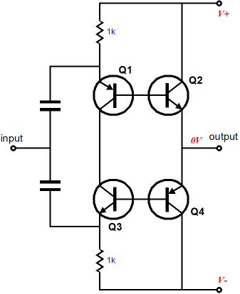
In the above schematic, we see only two cathode resistors, one per output device. The cathode resistor’s value must be carefully chosen, as we must reduce each tube’s transconductance by half. By dividing the triode’s rp by the sum of its mu + 1, we get the needed resistor value. (With pentodes, 1/gm is good enough for government work.) The unbypassed cathode resistor effectively increases the tube’s plate resistance by (mu + 1)Rk, so the total effective plate resistance is equal to rp + (mu + 1)Rk. At idle and at low signal levels, while the output stage still runs in class-A, the super-fast rectifiers never conduct, so the two output tubes effectively work in tandem, thereby doubling their halved gm back to their intrinsic gm. But once the output stage leaves class-A operation, the rectifier on the active tube’s cathode will conduct, thereby bypassing its cathode resistor. In other words, while the tubes are both engaged, their gm is halved, but once one cuts off, the other has its full gm restored. The zener’s break voltage must equal twice the cathode voltage at idle (with some tweaking as needed).
Class-AC Impedance Multiplier Circuit
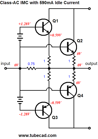
The above schematic shows an IMC that still runs class-A for the first 16W of power output. (Using larger emitter resistors will drop the idle current. In fact, 100-ohm emitter resistors can be used in a line-stage amplifier or headphone amplifier.) If 1-ohm emitter resistors are used the idle current drops to 590mA, which guarantees a class-A envelope of at least 4W, within which 90% of music will unfold. And with 45V to 50V power supply rails, something close 100W into 8-ohm load should be possible. Wouldn’t it be wonderful if amplifiers were specified with a dual power rating, for example 4W/100W.
The biggest problem is that of establishing the optimal bias voltage. I would certainly take a look into the ThermalTrak transistors from ON Semiconductor, as their internal diode could be used in setting up a self compensating voltage reference for the output transistors.
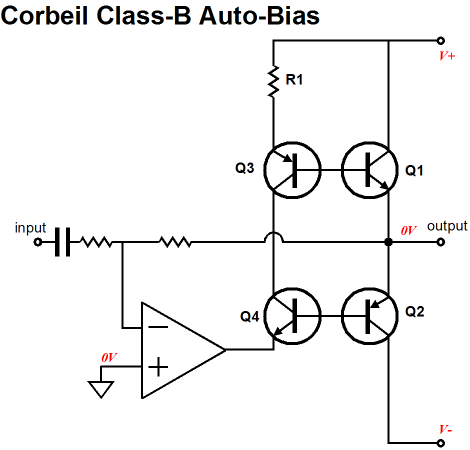
Pierre Corbeil, of Paradox Innovation in Montreal, Canada, certainly has earned his $150. EDN (Electronics Design News) magazine rewards submissions of design ideas with a check for $150 and all the glory that comes from seeing one’s name in print (or is only pixels these days?). His super clever design overcomes one of the huge problems with class-B amplifier design: getting the bias right—over time and over device heating. Too little bias and the amplifier falls into class-C and high distortion; too much bias, the amplifier overheats, possibly blowing a fuse. Many complex and finicky circuits have been devised to overcome the class-B transistor amplifier’s bias problems. Mr. Corbeil has come up with a clever auto-bias scheme that automatically adjusts the idle current through the output stage devices. By driving the two main output stage power transistors indirectly with two smaller transistors, the idle current through the is set by the current flow through resistor R1.
The smaller in value R1 is, the greater the current flow; the larger, the less the flow. Be sure to download the PDF and read his entire article. The sad irony here is that soon all solid-state amplifier will be of the class-D family, so Pierre's mad fast-ball comes a bit late to a baseball game that is already finished. For example, it appears that class-D has been married to class-G, giving birth to super-super efficient power amplifiers; the Audium AS1001 100W mono amplifier seems to be a good example.
Returning to Mr. Corbeil's circuit, what could be of use to us tube-loving folk is a unity-gain buffer made up from Corbeil’s class-B topology? Think hybrid power amplifier (or Moskido).
Next Time
//JRB |
E-mail from GlassWare Customers
High-quality, double-sided, extra thick, 2-oz traces, plated-through holes, dual sets of resistor pads and pads for two coupling capacitors. Stereo and mono, octal and 9-pin printed circuit boards available.  Aikido PCBs for as little as $24 http://glass-ware.stores.yahoo.net/
|
|||


| www.tubecad.com Copyright © 1999-2009 GlassWare All Rights Reserved |