| John Broskie's Guide to Tube Circuit Analysis & Design |
|
25 March 2018 Post 417
Brazil OTL Update
Balance is essential in both push-pull amplifier design and in life. Butterflies display their beautiful wing markings not to dazzle us, although they certainly do dazzle, but to allow the female butterfly to judge her potential mate's genetic suitability, which can be vouchsafed by perfect balance between wings. Ovulating women prefer the scent of more symmetrical men, i.e. men who exhibit low fluctuating asymmetry (FA). In the dark, all cats might be gray, but not all men are equally symmetrical. What about women and symmetry?
See post 300. In addition, the phenomena of beer goggles is easily explained by alcohol's baneful ability to short-circuit our ability to discern symmetry.
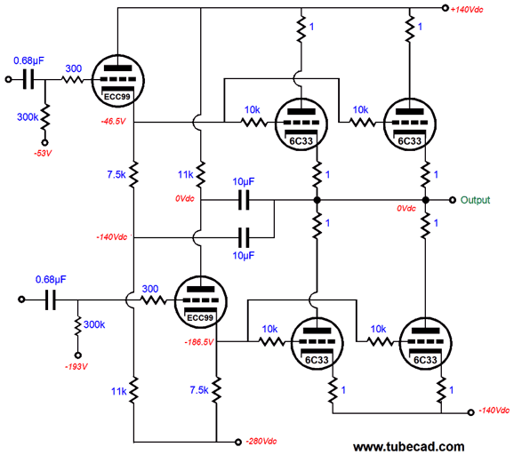
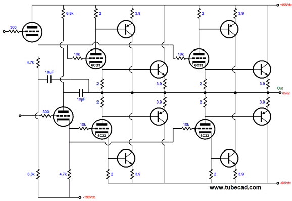
In the Brazilian OTL, the grids of the output tubes are DC coupled to two cathode-follower driver stages. Each cathode follower must see equal cathode-to-plate voltage and plate current swings, to ensure balanced drive of the output stage. The bottom cathode follower drives the bottom output tubes and its plate is in series with an 11k plate resistor that is AC tied to the output through a 10µF capacitor. As this cathode follower's cathode voltage swings negatively, the OTL's output swings positively. In contrast, the top cathode follower drives the top output tubes and its plate is tied to the 140Vdc power-supply rail. As the OTL's output swings positively, the link between its two cathode resistors moves up positively by the same amount due to the 10µF that ties that connection to the output. The net result is that both cathode followers do the same amount of work and experience identical -but anti-phase- cathode-to-plate voltage and plate current swings. By the way, I should point out that this assumes that music—not constant, prolonged test signals—will be the signal source, as the driving at the OTL at full output in a steady manner will end up disrupting the balance, as the cathode followers will be forced to absorb the positive-grid current from the output tubes, which will alter the 10µF capacitors' normally fixed voltage drop. True, some music does approach steady sinewaves from a function generator, say some electronic music (and possibly some organ music), and the modern Loudness War might also weaken the balanced operation. But as they say in the computer world, garbage in…
As I surveyed the revised schematic for other imbalances, my attention was drawn to the 6C33 cathode resistors. True, top and bottom cathode resistor all match, being 2 ohms in value. But the top cathode resistors also attach to the NPN transistor bases, while the bottom cathode resistors only attach to the bottom triodes' cathodes. A break in symmetry. The break is necessary, as the transistors get their own lower-voltage power-supply rails, a full hundred volts lower than the output triode's power-supply rail voltages. Now does this break in symmetry count? Since the transistors run in class-C and only turn on once the output triodes leave class-A operation, how troubled are the top triodes by the extra load imposed by the bases when the transistors turn on? A dang good question.
I have recently discovered that I have a leaky memory, which doesn't mean that data goes in and then drips away, leaving nothing behind. Instead, when I try to recall some information, a trickle of data pours forth; then more and more, and then even more.* Well, three-year-old memories dripped back into my mind. I had thought the exact same thoughts before.
Auto-Bias MOSFET Power Amplifier
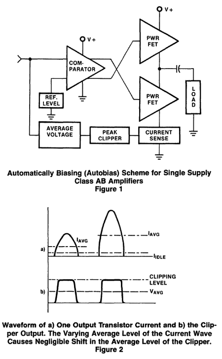
The following schematic appeared in an article titled, A New (AC Coupled) Topology for Automatically Biased Audio Amplifiers Using Power MOSFETs.
Note that the top MOSFET finds a diode and two resistors at its source. Why? When I first saw the schematic, I assumed that it was some sort of complementary-distortion canceling circuit—and I was sort of right, but not entirely. This amplifier uses a DC clipping circuit on the bottom MOSFET's source to sample the idle current flow through the output stage. The auto-bias feature uses the input differential input stage to set the idle current through the output MOSFETs to the value needed to establish a voltage drop across the bottom 1-ohm source resistor equal to one half the voltage needed to forward bias the 1N5391 diode (D3). As the amplifier amplifies, the output current will certainly exceed the idle current, so this diode will become forward biased a begin conducting. The result will be a square wave with rounded edges that cascades into the 82-ohm resistor and there it finds a 1N4148 diode terminating into ground, which will further sharpen up the resulting square wave, before sending it to an RC filter (10k resistor and 1µF capacitor), whose DC output voltage goes on the input stage for comparison to a voltage reference.
All in all, a very clever circuit, but one difficult to see due to the way the schematic was drawn. Once I figured out how it worked, the first thought I had was, "Hey, can't this same auto-bias technique be applied to tubes?" It can. The more I thought about this amplifier design, the more I wondered about the extra diode and resistor at the top MOSFET's source. Why were they there? My answer was that the significant portion of the clipping circuit below (the 1 and 0.68 ohm resistors and 1N5391 diode) was applied to the top MOSFET's source to restore balance. I could see how it was put there, but I wondered if it was wise to further balance in this way. For example, say you lost your left hand's pinky finger in an accident, should you then have your right hand's pinky finger amputated to restore balance? As I saw it, it was too bad that the bottom MOSFET had to work into a non-linear source resistance, so why do the same for the top MOSFET? I also wondered why a 0.68-ohm resistor was placed series with the diode, not a 6.8-ohm or 68-ohm resistor. Silicon diodes do not need amperes of current to become forward biased, requiring only sufficient voltage and a trickle of current. There had to be a reason behind the extremely low-valued resistor. Well, this was the seed that got me thinking about gm doubling and its removal years later. Imagine that the MOSFETs offered infinite transconductance. Such a MOSFET working with an unbypassed source resistor will exhibit an effective transconductance equal to the inverse of the source resistor's value. In this example, the 1-ohm source resistor reduces the infinite transconductance to 1A/V. (If we could buy a triode with a transconductance of 1A/V, we would be thrilled beyond words.) But as the MOSFET's current conduction increases sufficiently to forward bias the diode, the 0.68-ohm resistor becomes effectively in parallel with the 1-ohm resistor, resulting in a combined resistance of 0.4 ohms. With this lower source resistor value, the infinite-gm MOSFET's transconductance increases to 2.5A/V. Of course, no MOSFET offers infinite transconductance. The formula for the resulting transconductance with an unbypassed source resistor is gm' = gm / (1 + gmRs) Unfortunately, the 1N5391 was a poor choice, as it is suuupper sloooow (1500 ns). An ultra-fast rectifier is a better choice, many being over 40 times faster. I believe if they had used a faster diode, they might have been prompted to dig a little deeper into what was behind that ratio. In the article, the authors refer to the diode performing a dynamic bypassing of the 1-ohm source resistor, which is the first step to understanding how a constant-transconductance output stage can be made. Rereading this over 30 year-old article reminded me of Neils Bohr in 1913 rereading his 28 year-old physics textbook and seeing Balmer's spectral formula again (or for the first time) and realizing how light's frequency corresponded to the different energy gaps between the fixed electron orbits he had postulated (and with Plank's constant thrown in). In other words, when I first read the article, I wasn't thinking about gm-doubling at all. Today, I am thrilled that the authors' empirically derived ratio matched my mathematical model's prediction exactly. This memory was then pushed aside by a new torrent memories.
Hybrid Headphone Amplifier
Remember the great scene in the great movie, The Flight of the Phoenix, where James Stewart's character discovers -—to his horror—that the airplane engineer, the one who is designing their escape airplane, has only designed model airplanes, not big aircraft. Topology is topology; scale does not enter the picture.
Origami requires a square sheet of paper, but the size of the paper is up to you; nonetheless, the same shape results no matter how small or how big. Although this design uses an ECC99, theere is no reason why it could not be scaled up to use two 6C33 or 300B tubes.
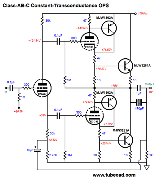
This circuit runs the triodes and the PNP transistors in class-AB, while the NPN transistors run in class-C, which we never encounter in 99.99999% of audio amplifiers. (Sorry for leaving off the last 99999999 digits, but my fingers were getting tired.) Class-C means that the NPN transistors are completely turned off at idle and only turn on during part of the sine-wave output, if at all. As long as the output stage operates within the confines of class-A operation, the NPN transistors remain turned off. They only turn on when their partnered triode doubles its idle current conduction, which means that the opposing triode has ceased conducting. Once a NPN transistor turns on, it effectively doubles its partnered triode's transconductance. The result is a constant-transconductance output stage, so gm-doubling does not arise. What do the PNP transistors do? They form a compound amplifier topology with their partnered triode. The triode is in charge and it controls its PNP transistor. The result is greatly lower distortion and output impedance. Once the triode's current conduction falls below the value needed to develop a base voltage great enough to keep its PNP transistor turned on, the transistor turns off. Effectively, the PNP transistor strives to maintain a fixed current flow through its partnered triode. In other words, a low volume, both the triode and PNP transistor do all the work of driving the low-impedance load. But as the output current rises, the triode's current conduction flat-lines and the PNP does most of the heavy lifting, with only occasional help from the NPN transistor. This hybrid, class-AB-C output stage must be driven by a "smart" phase splitter, which means a phase splitter that incorporates the output signal in its development of the needed asymmetrical pair of output signals to achieve a symmetrical output swing. (Remember, the top triode must see a larger drive signal than the bottom triode, as its cathode swings up and down with the output signal.) We could use either a long-tail phase splitter or a split-load phase splitter. The latter is shown in the following schematic.
The 1kµF (1mF) capacitor returns the output signal to the split-load phase splitter, which effectively results in both output triodes operating as grounded-cathode amplifiers. If this is not clear, imagine a 1Vpk positive pulse forced upon the output. This pulse would force the top output triode's cathode 1V up, while it also forced the split-load phase splitter's plate output up by 1V. In other words, the top triode would only see its cathode-to-plate voltage fall by 1V, while its cathode-to-grid voltage would remain unchanged. The bottom triode, on the other hand, would not see any cathode-to-grid voltage change, but it would see its cathode-to-plate voltage rise by 1V. In other words, both triodes would only offer their plate resistance to oppose the positive pulse. If we add an input stage and negative feedback loop, the pulse can be countered much more aggressively by both output triodes. Just two tubes (a 12AX7 and a ECC99) and four transistors (MJW1302A and MJW3281A) are required per channel.
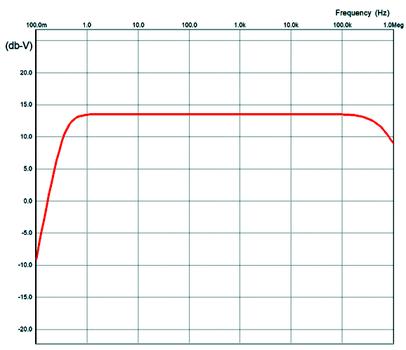
That same 1V positive pulse enters the input triode's cathode through the 1kµF capacitor and 2k feedback resistor. The input triode responds by decreasing its current conduction, as its grid is effectively now more negative relative to its cathode. Thus, its plate voltage increases, due to the smaller voltage drop across its plate resistor. This upward voltage swing is then relayed to the split-load phase splitter, whose top output swings negative and its bottom output swings positive, which forces the top triode's current conduction to fall and the bottom triode's conduction to rise, both serving to counter the externally applied positive pulse. By the way, often coupling capacitor values are pulled out of the air (or some other word that begins with an "a"). Not this time. All the internal and output coupling capacitor values were chosen to yield a flat frequency response in SPICE simulations. Note how the 1kµF capacitor does not attach before the output capacitor, but after it. My original values produced a bass hump below 20Hz. The above values produced this plot line.
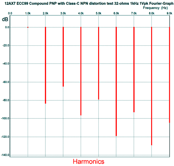
How well does this elaborate scheme work? Very well indeed, thank you very much. Here is the SPICE-generated Fourier graph of the harmonics resulting from a 1kHz output at 1Vpk into 32-ohms.
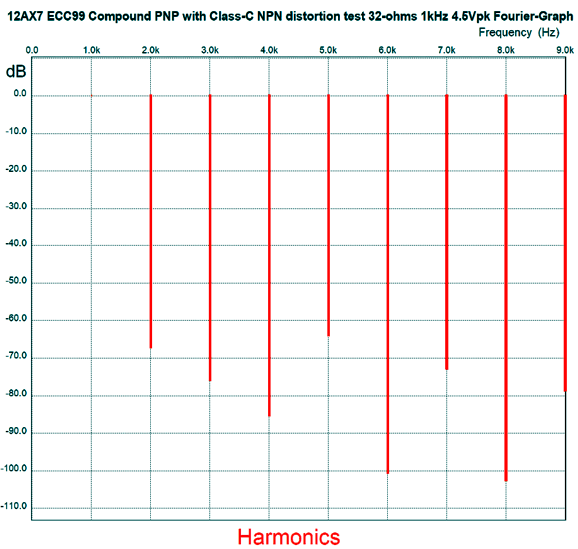
Not bad at all. Here is the graph for 4.5Vp of output (1Vpk of input signal).
Yes, the 3rd harmonic went down, not up. As can be seen, the added transistors serve to supercharge the output triodes. What if we do away with all the transistors? Pure tube for pure hearts and pure ears? Well, we won't get the full output, as only 3.5Vpk develop with 1Vpk of input signal. Here is the resulting Fourier graph.
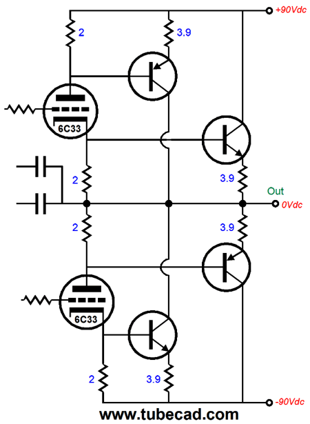
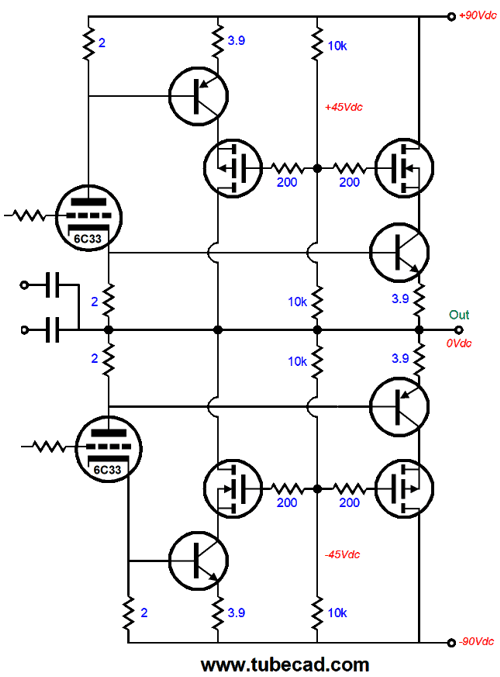
The distortion comes in at a tad over 1%, whereas it had been about 0.1% with the transistors. Well, the next question is: Can this topology be used in a power OTL for driving loudspeakers, not headphones? Yes, but we can take either half of it or all of it. By half of it, I mean that we can run the output tubes in class-AB, while all the transistors run in class-C, as shown below.
Why only class-C? Note the +/-90Vdc power-supply rails. If a transistor idled at the same 150mA that each 6C33 triode idles at, it would dissipate 13.5W at idle, toasty hot for a transistor. If it experienced a peak current flow of 1A, however, it would dissipate a vastly higher instantaneous wattage and go up in flames. In contrast, if the transistors are completely turned off at idle and if the music played is interesting enough to display a large dynamic range, then the transistors will only conduct when needed to fill in the missing current from one set of output tubes cutting off and they might survive. Here is the phase splitter and output stage.
Unlike the Brazilian OTL design, the power-supply rails here are only 60% as high in voltage (+/-90V versus +/-140V), but over twice as high as the Brazilian OTL's transistor power-supply rail voltage. Couldn't we use power MOSFETs instead? Certainly, but the problem with MOSFETs, although they tend to prove much more reliable in actual use, is that they require a much higher turn-on gate voltage and this voltage is not nearly as fixed as the transistor's turn-on base voltage. We could, however, use MOSFETs in a cascode arrangement.
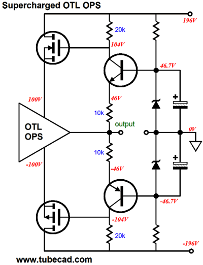
If we could deliver 80Vpk of output voltage swing into an 8-ohm load, we would get 400W of output. Now, if you were to build a 400W solid-state power amplifier, you would use dozens of output transistors and a truly huge heatsink. On the other hand, if we limit the transistors to class-C, as shown in the above schematic, we might be able to get away with fewer transistors and smaller heatsinks. In the above schematic, each output triode gets two slave transistors that run in class-C. Each transistor will conduct half of the require current to double its master triode's transconductance when the opposing triodes shut off and the output stage leaves the class-A window of operation. The transistors are rated for 200V, which is dangerously close to the combined +/-90V power-supply rail voltages, 180V. Replacing one transistor with two MOSFETs or two transistors in cascode would both halve the dissipation and double the voltage limit. This arrangement would allow us employ the expanding power-supply-rail-voltage solution that I proposed back in post 288, which gives the tube-based OTL output stage lower power-supply rail voltage at idle, then as the output swings away from 0V, the power-supply rail voltages expand further. In other words, not class-G, but supercharged class-G. Why? The analogy I made before was that of a magic wallet, a wallet that fills with more money than you pull from it. Take out a twenty and two take its place. Well, the more power-supply rail voltage we give the output triodes, the more current can flow from them.
Okay, what if we want not half, but all of the headphone amplifier topology, where the PNP transistors conduct at idle; in fact, they conduct more current than the output triodes. At idle, the NPN transistor run in class-C and are completely turned off. This might prove the best way to go, as have more options available to us, and the more current we can outsource to the solid-state devices, the more output power we can realize. Here is an example of more options. Since the PNP transistor are conducting at idle, we are not strictly wedded to bipolar transistors. P-channel MOSFETs with -250V voltage limits and 150W power rating cost less than $2 each (FQA9P25).
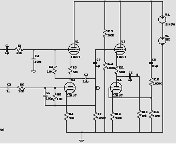
After this long and twisted path, I returned to the Brazilian OTL output stage with the +/-40V power-supply rails for the transistors and the apparent imbalance between the source load seen by top and bottom output triodes. Maybe a workaround could be found in using Darlington transistors to drive the power transistors? Maybe, just maybe, there was no major imbalance. I created the following SPICE circuit to see what was going on between top and bottom output triodes.
Yes, I know it doesn't look like the Brazilian output stage. It does not have to, as SPICE is an abstracted world. Effectively, this arrangement of parts reveals what goes on in the Brazilian OTL output stage. The triodes still see a 140V cathode-to-plate voltage, while the transistors still see a 40V emitter-t-collector voltage. We then sweep the 6C33 grid voltage from -80V to +10V and compare the two resulting plate-current plot lines.
Two plot lines are shown, but they overlap so well that it looks like only one plot line is shown. I ran many more SPICE simulations on variations on this circuit. These further simulations revealed that the asymmetrical driving of the output transistor from cathode with the top triodes and from the plate from the bottom triodes did add a tad more distortion, but this extra distortion was far below what the triodes on their own contributed that it could safely be ignored.
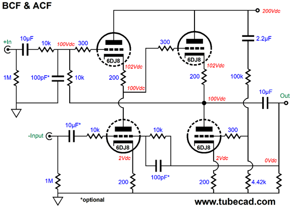
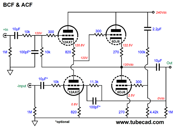
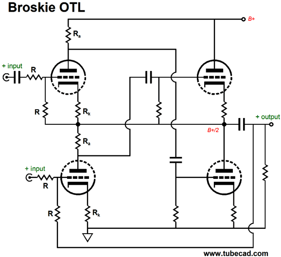
Four-triode Broskie Cathode Follower
Interesting. A BCF cascading into an ACF. I would do it differently:
Not only do we eliminate one internal coupling capacitor, but the ACF's low-impedance output drives the feedback loops. We do not have to use the same tube throughout.
Note the 12AX7 BCF tube and the 240Vdc B+ voltage. This circuit performs quite well in SPICE simulations. The 11.3k feedback resistor was used to improve the CMRR of the circuit. The question is, Does this perform any better than the Broskie OTL circuit?
Blog post numbers, 193, 194, 196, 239, and 249 give the details.
//JRB
*Leaky Memory Here is another example, recently my teenage son asked me what I knew about Ovid. My answer: "nothing." Well, I did know that he was an Ancient Roman poet. In fact, I have even memorized a long quote from him in Latin, although I don't speak Latin, but I liked the quote from his Metamorphosis so much that I long ago committed it to memory. As I was proclaiming my ignorance of Ovid, however, I recalled that he had been implicated in the emperor Augustus's daughter Julia's banishment for her scandalous sexual conduct and that Ovid had been banished to some remote Roman outpost, somewhere near Romania, where he was as miserable as Oscar Wilde would have been had he been banished to the American Mid-West, which was evidenced by Ovid's many pleading letters to later emperors asking for forgiveness and a ticket back to Rome. Then I remember that, like Lucretius, he also had been deeply Greek influenced, and that Ovid had possibly—no, more like probably—had studied in Greece, but that, unlike his contemporary, Lucretius, who had written a very noble but stiff Latin poetry, Ovid had managed to break his Latin verse out of its unbendable confines and written a much more fluid poetry—and that he might be partially responsible for making modern Latin-based languages, such as Italian, French, and Spanish more pliable as a result; and, finally, I recalled that his poetry had helped fuel the Renaissance, as what could be more fun that high-brow sex-filled literature? Shakespeare, Spencer, and Milton loved Ovid. In other words, just as I told my Son: I don't know anything about Ovid. Or, put differently, the memories are there, but they take time to gather and flow back into my consciousness.
User Guides for GlassWare Software
For those of you who still have old computers running Windows XP (32-bit) or any other Windows 32-bit OS, I have setup the download availability of my old old standards: Tube CAD, SE Amp CAD, and Audio Gadgets. The downloads are at the GlassWare-Yahoo store and the price is only $9.95 for each program. http://glass-ware.stores.yahoo.net/adsoffromgla.html So many have asked that I had to do it. WARNING: THESE THREE PROGRAMS WILL NOT RUN UNDER VISTA 64-Bit or WINDOWS 7 & 8 or any other 64-bit OS. I do plan on remaking all of these programs into 64-bit versions, but it will be a huge ordeal, as programming requires vast chunks of noise-free time, something very rare with children running about. Ideally, I would love to come out with versions that run on iPads and Android-OS tablets.
//JRB
|
|
John Gives
Special Thanks to the Special 69
I am truly stunned and appreciative of their support. In addition I want to thank
All of your support makes a big difference. I would love to arrive at the point where creating my posts was my top priority of the day, not something that I have to steal time from other obligations to do. The more support I get, the higher up these posts move up in deserving attention. Only those who have produced a technical white paper or written an article on electronics know just how much time and effort is required to produce one of my posts, as novel circuits must be created, SPICE simulations must be run, schematics must be drawn, and thousands of words must be written. Only those who have produced a technical white paper or written an article on electronics know just how much time and effort is required to produce one of my posts, as novel circuits must be created, SPICE simulations must be run, schematics must be drawn, and thousands of words must be written.
If you have been reading my posts, you know that my lifetime goal is reaching post number one thousand. I have 583 more to go. My second goal is to gather 1,000 patrons. I have 931 patrons to go. Help me get there.
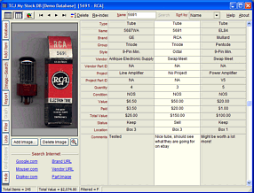
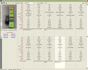
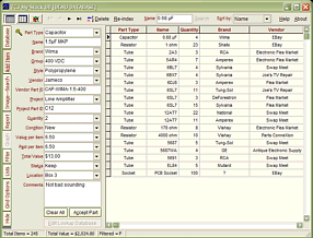
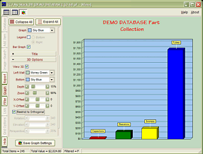
Only $12.95 TCJ My-Stock DB
Version 2 Improvements *User definable Download for www.glass-ware.com |
||


%20Topology%20for%20Automatically%20Biased%20Audio%20Amplifiers.png)


| www.tubecad.com Copyright © 1999-2018 GlassWare All Rights Reserved |