| John Broskie's Guide to Tube Circuit Analysis & Design |
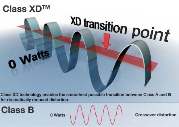
02 December 2006 Amplifier Class-XD™
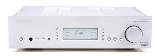
“Another day, another dollar.” No, wait—I meant to say: “Another catalog from Audio Advisor, another misleading entry for the Vincent SV-236 integrated amplifier.” This 100W class-AB amplifier is once again billed as a “100-Watt Integrated Amp with Pure ‘Class A’ Output Stage.” The unfortunate truth is that this amplifier can only put out 10-watts of class-A output (pure or impure) before it enters class-B mode. Considering that the intended customers are audiophiles, however, we should be thankful that the copy offered only a single magnitude of exaggeration, not the usual hundredfold increase in hype. (By the way, I am often asked if Stereophile magazine has asked me to write for them. My answer has always been that the editors of Stereophile do not know that I exist. Even if they did, surely the previous paragraph alone would be enough disqualify me from consideration.) Back to the catalog, on page 60, I found a new integrated amplifier from Cambridge Audio, the Azur 840A, a $1,375, 120W effort that “Redefines Affordable Hi-End” by employing a new amplifier class of output stage mode—class XD™.
Normally, I would ignore such copy, but as I own a Cambridge Audio Azur 640C v2 CD player (which I like and which I bought from Audio Advisor) and since the 840A was so clean looking, I was intrigued enough to look into this new development. From Audio Advisor’s website, we learn:
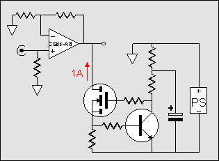
Interesting, very interesting. Although a new product, the 840A has already won many recommendations and awards, including the CES Innovations 2007 Award for Design and Engineering. (Which is truly impressive considering that we are still living in the year 2006.) So, what is class XD™ and how did they do it? The white paper at Cambridge Audio's website reveals the important details, including that Douglass Self, whom I much admire, now works for Cambridge Audio and that the XD project took two years to come to fruition. But before you read the whitepaper’s many pages, you should read just one page I wrote almost five years ago in the Tube CAD Journal. There you will find the following schematic.
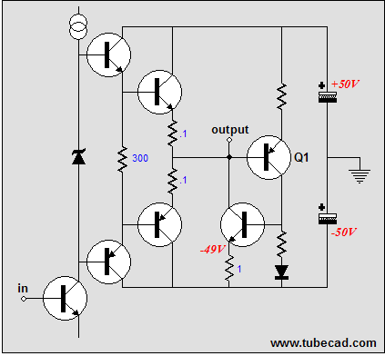
(Forgive the GIF image; now, you can see why I switched to PNGs.) The constant-current source undoes the amplifier’s push-pull operation over the output voltage swing defined by the constant-current source’s idle current against the load impedance; thus, for example, 1A and 8-ohms define a range of +/-8 volts. Inside this limited voltage swing, the output stage runs in single-ended, class-A mode (AKA, patent-pending class-XD™). Outside this range, the amplifier reverts to class-B, push-pull operation. The great advantage this topology brings is that the dreaded crossover notch distortion occurs well away from the zero crossing, where the ear is most sensitive. (Image if the steering wheel in your car stuck a bit at the exact center of its turning range, as opposed to just sticking only during tight u-turns.) Now, from the Cambridge Audio whitepaper, we learn that the new Cambridge Audio's patent-pending-proprietary-XD™ technology adds a slight twist: the constant-current source’s current is not constant; instead, the current varies with the output swing, drawing the most current when the output swings down close to the negative rail voltage, and drawing the least current when the output swings close to the power supply rail voltage. The formula that the whitepaper specifies is The above schematic shows a PNP transistor Q1 nestled in the output stage, with its base attached to the output, and its emitter and collector terminated into resistors. The bottom resistor is placed in series with a signal diode to compensate for the base-emitter voltage drop. The top resistor attaches to the positive power supply rail. Thus, when the output swings positively, the voltage across the resistor and the current through the resistor decrease; which, in turn, decreases the voltage across the bottom resistor, forcing the current source’s current draw to fall. Conversely, when the output swings negatively, the voltage across the resistor and the current through the resistor increase; which, in turn, increases the voltage across the bottom resistor, forcing the current source’s current draw to climb. No doubt that with a glass of port and ten minutes, an OpAmp-based circuit could be designed that would achieve the same function. But what if I don’t want to use a sliding bias current? Longtime readers will remember my disinclination to make an active load too active. Actually, here is the irony of the situation: John Atwood recently gave me an early Christmas present in the form of matched pairs of ON Semiconductor ThermalTrak power transistors (NJL3281D and NJL1302D). This gift has compelled a rethink on the Class-A-SE/Class-AB-PP amplifier. The problem with using a constant-current source as the active load is that it will dissipate a lot of heat when the output swings to the positive rail. Because the current conduction is constant, the current source's dissipation is linear against output voltage swing: 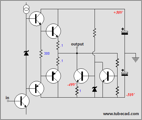
In the schematic above, we see how easy it is to set a threshold voltage and turn off the constant-current source. When the output voltage swings positively enough to turn on transistor Q2, the transistor’s collector will pull down heavily, forcing transistor Q1’s bias-reference voltage to collapse, switching transistor Q1 off. Another path around the crossover distortion might be to follow Vincent’s lead and build a richly biased class-AB amplifier. Like the Vincent SV-236 integrated amplifier, such an amplifier would run in push-pull class-A for the first 4W, let’s say, thereafter it would enter class-B mode. The problem with this approach is that the large overlap of conduction results in transconductance doubling, wherein the distortion and output impedance climb after the transition is made to class-B. Below is an interesting workaround that I have been playing with. 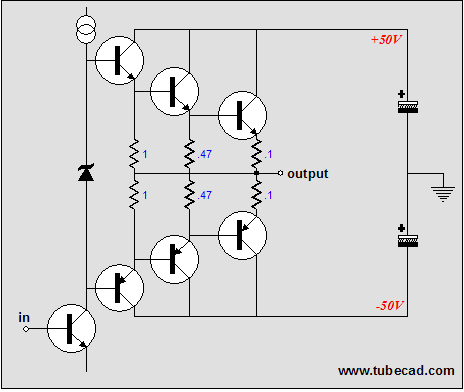
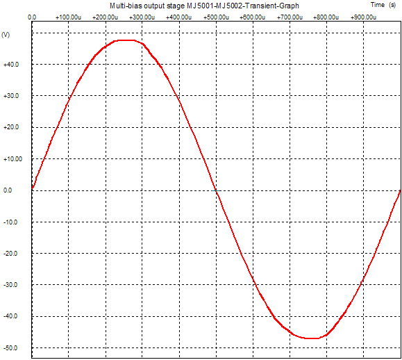
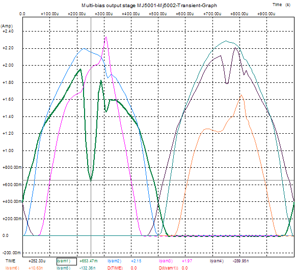
At idle, with no input signal, only the leftmost output transistors conduct. As the output swings far enough away from 0-volts, the second set of transistors engage; then after even greater current delivery into the load, the final set of transistors turn on. What we have done is swap one crossover glitch for four glitches; but as none fall within the first four watts, the trade was a wise one, as the all the output transistors run below their beta-droop threshold. Additionally, and perhaps most importantly, this output stage clips softly, as the secondary transistors turn off as the voltage ceiling is approached. Below is a SPICE simulation of the output stage's output, after seeing a 50Vppk input signal. Not bad, particularly when compared to a flat-topped sinewave. The current flowing through each output transistor looks much worse.
As I have said before, all amplifiers clip; some do it gracefully, whereas others clip harshly and shrilly. How an amplifier clips is vital, but most often overlooked. But not always, as a new IC power amplifier from Maxim has been designed to clip softly. The MAX9756 is a 2.3W amplifier that includes an ALC (automatic level control) in its small package. This added circuit rounds off the square waves that the average amplifier would create, resulting in a much more listenable amplifier for laptops and portable DVD players. I am sure that in a shootout, the MAX9756 would sound much more powerful than its 2.3W rating would imply.
//JRB
|
Only $12.95
Download or CD ROM www.glass-ware.com
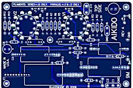
High-quality, double-sided, extra thick, 2-oz traces, plated-through holes, dual sets of resistor pads and pads for two coupling capacitors. Stereo and mono, octal and 9-pin printed circuit boards available.  Aikido PCBs for as little as $24 http://glass-ware.stores.yahoo.net/
The TCJ Stepped Attenuator The center knob controls both channels, and offers six large decrements; the flanking knobs offer six fine decrements for each channel, creating a volume control and balance control in one easy-to-use stepped attenuator. This clever attenuator uses fewer resistors (only 32) than would be expected from a conventional 32-position stepped attenuator, as two series attenuators would need a total of 72 resistors; and two ladder attenuators would require 140 resistors. In addition, the PCB holds dual sets of resistor pads, one wide and one narrow, so that axial (composition, wire-wound, and film) and radial (thick-film and bulk-foil) resistors can be used without extra lead bending. Although designed to go with the Aikido amplifier, it can be used anywhere a high-quality attenuator is needed, whether passive or active. For example, it would make a first-rate foundation to an excellent passive line box. Visit our Yahoo Store for more details: http://glass-ware.stores.yahoo.net/
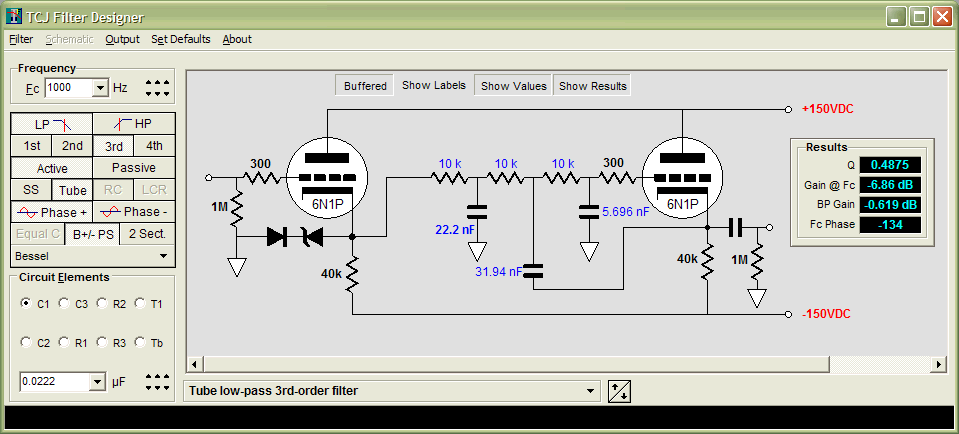
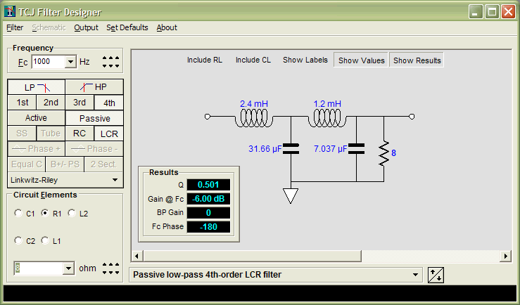
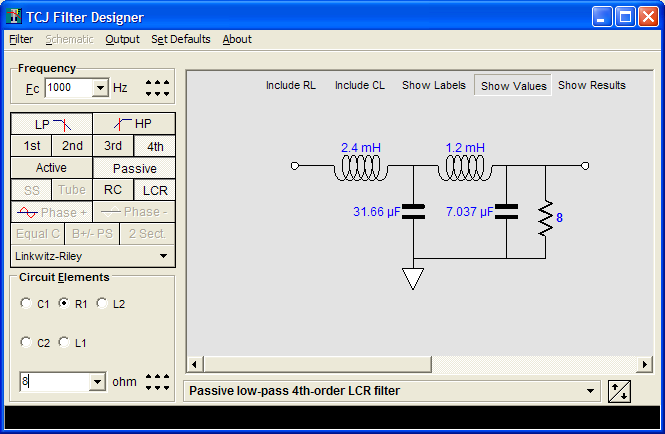
The Tube CAD Journal's first companion program, TCJ Filter Design lets you design a filter or crossover (passive, solid-state or tube) without having to check out thick textbooks from the library and without having to breakout the scientific calculator. This program's goal is to provide a quick and easy display not only of the frequency response, but also of the resistor and capacitor values for a passive and active filters and crossovers. TCJ Filter Design is easy to use, but not lightweight, holding over 60 different filter topologies and up to four filter alignments: While the program’s main concern is active filters, solid-state and tube, it also does passive filters. In fact, it can be used to calculate passive crossovers for use with speakers by entering 8 ohms as the terminating resistance. Click on the image below to see the full screen capture.
Tube crossovers are a major part of this program; both buffered and un-buffered tube based filters along with mono-polar and bipolar power supply topologies are covered. Available on a CD-ROM and a downloadable version (4 Megabytes). Download or CD ROM
|
|||


| www.tubecad.com Copyright © 1999-2006 GlassWare All Rights Reserved |