| John Broskie's Guide to Tube Circuit Analysis & Design |
| Post 218 15 November 2011
V-to-I Power Amplifiers (Current-Output Amplifiers)
I know many readers are wondering why I am spending so much time on this topic, particularly as V-to-I amplifiers are so rare. My answer takes two forms. The first is that the V-to-I amplifier may become much more popular in the future, so it cannot hurt to get ahead of the pack. Second is that because the V-to-I amplifier inverts so much of what we imagine is absolutely permanent, fixed, irreversible, and, indeed, irrevocable about amplifier design, it is a useful source of mind-stretching material. For example, with modern voltage-output amplifiers that boast of output impedance of in the milliohms, setting a coupling capacitor's value is straightforward: C = 1/(2 x pi x Frequency x Load Resistance), or C = 1/(6.28 x F x R). Given an 8-ohm load and a 20Hz low frequency cutoff, a 995µF (1kF) capacitor is needed. But what happens when the amplifier's output impedance is in the thousands of ohms? What size coupling capacitor is needed? Assuming a fairly low Zo of 1k (for a V-to-I amplifier) and an 8-ohm load, R becomes 1008 ohms, which when used in the preceding formula yields a value of only 7.9µF, not the 1kµF that you might expect.* Interesting, don't you think? And what about conventional crossovers and Zobel networks, do they still function with an I-to-V amplifier? And what about reactive speaker loads, such as prensent by piezoelectric tweeters? And what about output stage gm doubling issues? Do they still apply?
Zenlike I-to-V Power Amplifier
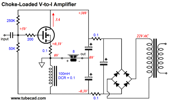
The maximum theoretical efficiency with a choke load would be 50%, which no real circuit can hope of achieving. With a constant-current-source load, the maximum theoretical efficiency drops to 25%. Thus, with an active constant-current-source load, at least 100W of idle dissipation would be needed to generate 25W into the speaker. Long ago Nelson Pass famously asked, What is the sound of one MOSFET amplifying? His answer was his Zen amplifier, a minimalist design that relied on the transconductance of a single output MOSFET to deliver all the needed voltage and current swings. His design was a V-to-V type that accepted an input voltage signal and produced a proportional output voltage swing. The following V-to-I amplifier (which first appeared in blog number 155 and is described fully there) produces a proportional output current swing.
What I love about this design is that will confuse just about everyone, yet is childishly simple. By the way, if a choke with a DCR in the milliohms, then the bottom capacitor at the amplifier's output would not be needed. Moving on to something more zen-like, the following circuit also relies on a single MOSFET (the bottom one) to provide voltage to current conversion. The top MOSFET replaces an inductor; but unlike an inductor, it gets hot, real hot.
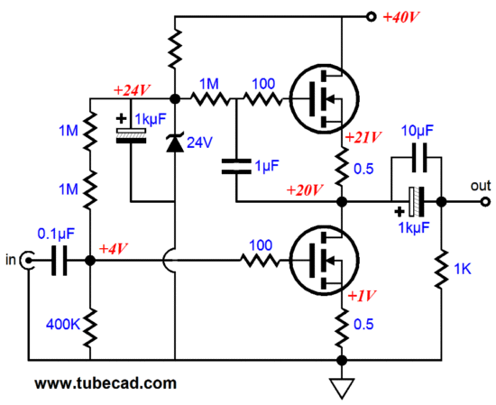
Like the Pass's Zen amplifier, this amplifier uses the bottom N-channel MOSFET's transconductance to do all the major work. The top MOSFET is configured in what I call a compliant constant-current source, as it is not set to any fixed amount of current flow, rather it adjusts to match the idle current through the bottom MOSFET and sets the DC division of the B+ voltage to 50% at the output. As far as I know, I am the only one championing this topology, which is odd, as this circuit works wonderfully well and is quite simple. The idle current is set at 2A, so 2A peak can be delivered into the load. If the load is 8 ohms, then the peak voltage across the load is 16Vpk and maximum wattage into the load is 16W. The dissipation at idle is 40V against 2A, 80W; this puts the amplifier efficiency at 20%. The big problem this amplifier presents is the heavy input capacitance. A 12AX7-based line stage is not going to cut it. One workaround is to add a PNP transistor in between the input and the MOSFET's gate, which allows the transistor's heavier idle current to charge and discharge the MOSFET's high input capacitance.
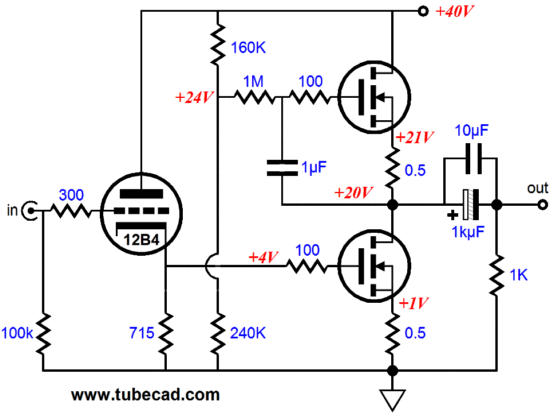
Or, if even one transistor is too many, the following tube-based hybrid could be made. Note the loss of the input coupling capacitor and the DC coupling of the MOSFET's gate to the 12B4 triode's cathode.
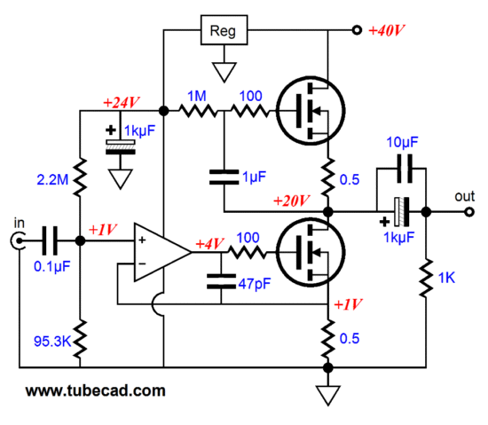
Which version do I prefer? This might surprise you, but I bet the PNP transistor beats the 12B4. Why? The problem with the 12B4 hybrid circuit is that two N-type devices, the triode and the N-channel MOSFET cascade in current phase, so both devices will compound in their similar nonlinearity, whereas the PNP transistor works in current anti-phase to the N-channel MOSFET, so their two nonlinearities tend to cancel. In other words, as the input signal swing positively, it works to diminish the PNP transistor conduction, while increasing the N-channel MOSFET's conduction. Not shown, in all the above schematics, are the trim potentiometers needed to set the desired idle current and center the output at B+/2. The following version uses an OpAmp to drive the MOSFET and automatically set the idle current through the output stage. A FET-input OpAmp would work best, as the OpAmp's inputs are quite close to the its negative rail voltage (ground potential, in this case). The AD823, AD825, OPA627, OPA637, OPA2132, OPA2604, come to mind.
Of course, if a negative power supply rail, say -5Vdc, were added for the OpAmp's benifit, just about any OpAmp could be used, as long as it was unity-gain stable. Note that the conversion ratio is 1V in equals 2A out. As far as the OpAmp is concerned, it configured as unity-gain power buffer, with a 0.5-ohm load. The next design is still single-ended, no matter how push-pull it may appear, so do not push the push-pull panic button yet.
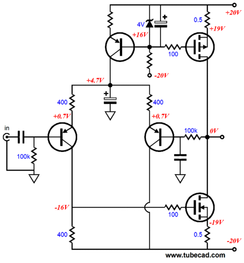
The P-channel MOSFET (at the top) is configured as a fixed constant-current source, which sets the idle current through the bottom N-channel MOSFET. The input stage, a long-tailed differential amplifier, is only a true differential amplifier at DC, as the AC signal is shunted away through the two capacitors. In terms of audio frequencies, all that is there is the input PNP transistor and its 400-ohm collector and emitter resistors. Since these two resistors match in value, the circuit becomes effectively a split-load phase splitter. I came up with this topology to allow me to drive the bottom MOSFET with an input signal referenced to the negative power supply rail, which the split-load phase splitter's abysmal PSRR figure makes possible. In other words, I wanted to achieve two goals: DC shifting the input signal and superimposing all of the negative power supply rail's noise on the input signal, so that the bottom MOSFET would be effectively blind to the noise, as both its gate and source would see the same noise signal. In terms of DC operation, the input long-tailed differential amplifier compares the output DC level to ground potential and adjusts the output to fall in line. Yes, we are back to the problem of the input PNP transistor and the N-channel MOSFET cascading in current phase, so both devices will compound their similar nonlinearity, but the other features of this design are so compelling, such as DC coupling at the output and the fixed idle current, that I would accept this as a necessary minor evil, besides the transistor will undergo smaller current variations in driving the bottom MOSFET, so it will produce less distortion than the 12B4 triode.
Simple Push-Pull I-to-V Power Amplifiers
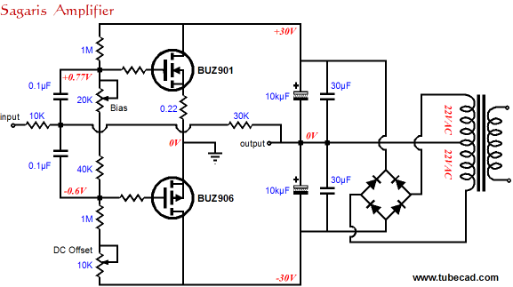
Well, with a little subtractive modification, this topology can be transformed into a V-to-I power amplifier.
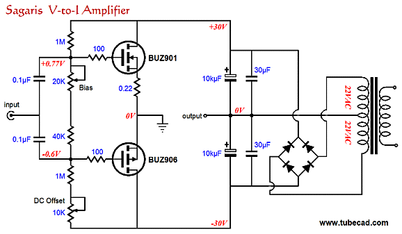
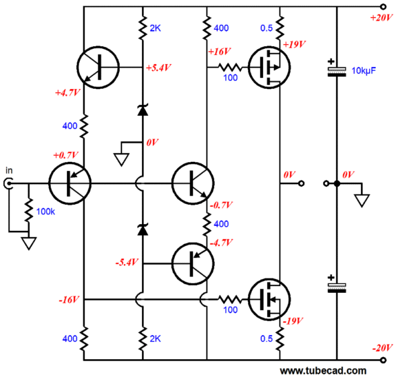
The BUZ901 & BUZ906 are lateral power MOSFETs that offer excellent linearity and fairly low input capacitance; unfortunately, they are both hard to find and expensive. Note how the removal of the feedback resistors (10k & 30K) radically changed the amplifier's output mode. The two 1M resistors only provide DC feedback, not AC feedback. Also note how each channel must have its own floating power supply, which of course would prove no big deal with a monobloc amplifier chassis. A move up in complexity is to borrow from the the previous single-ended V-to-I amplifier that made use of a long-tailed differential amplifier for DC operation and a split-load phase splitter for DC shifting of the input signal, the latter trick we will keep in our new push-pull amplifier.
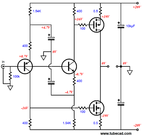
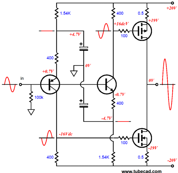
Once again we see transitor-based split-load phase splitters. In fact, the split-load phase splitters are used more as phase inverters than true phase splitters. The following schematic reveals the phase relationships within this V-t0-I amplifier.
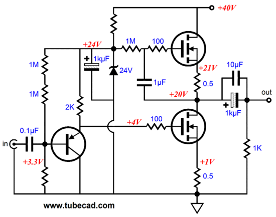
Note how both output MOSFETs see an inverted input signal relative to the signal presented to the entire amplifier. Also note how as the input signal swings positive, the P-channel MOSFET at the top increases in conduction, while the N-channel MOSFET at the bottom decreases in conduction, forcing the output to swing positively. Cute as this design is, it has some problems. The idle current is dependent on the rail voltages; as the rail voltage climb, so too the idle current. Second, the output may not center, as there is no DC feedback mechanism to keep the offset low. The following design overcomes the first problem.
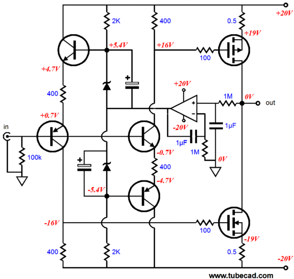
The zener diodes set a (roughly) fixed idle current, independent of the power-supply-rail voltage shifts. The problem of a non-centering output remains, however. The next modification solves that problem by introducing a DC servo loop, which monitors the DC offset and corrects any drifts away from zero volts.
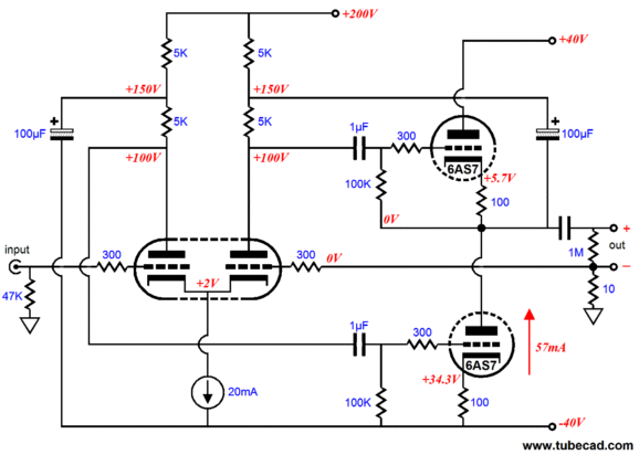
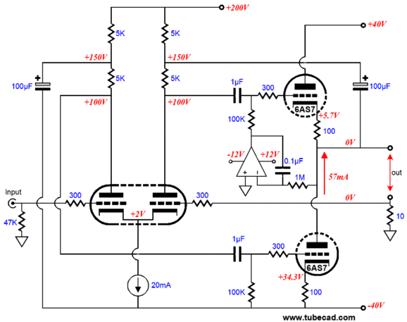
All-Tube PP OTL V-to-I Amplifier
I specified the 6AS7 dual triode just as a design example, but other hefty triodes could be used, such as the 6082 or 6C33 or 12B4 or 6S19... This amplifier works to maintain the exact same voltage superimposed on the 10-ohm resistor at the out as appears at the amplifier's input, which creates a voltage-to-current ratio of 1V to 100mA, which against a 50-ohm headphone driver, equals 5Vpk. Note how easy it would be to convert this V-to-I amplifier into a conventional V-to-V amplifier: just take the negative out at ground instead of the connection to the 10-ohm resistor and replace the 10-ohm and 1M resistors at the output with a 100-ohm and 1k resistors, which yield a voltage gain of 11.
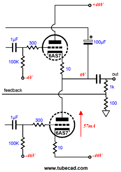
Since a goal of a voltage-output amplifier is a low output impedance, the 100-ohm cathode resistors have been replaced by 10-ohm resistors and negative bias voltages are used. (An alternative setup would be to use the top 10-ohm cathode resistor and a 100-ohm bottom cathode resistor with a large bypass capacitor, say 1kµF.) Returning to the original schematic, also note how the negative output is NOT grounded, which means that a balanced connector must be used with headphones, not the standard three element plug, as both headphone driver DO NOT share a common ground connection.
The coupling capacitor is there as a safety measure, as the DC offset may be up to a few volts off 0V. The following version uses a DC servo to keep the offset low.
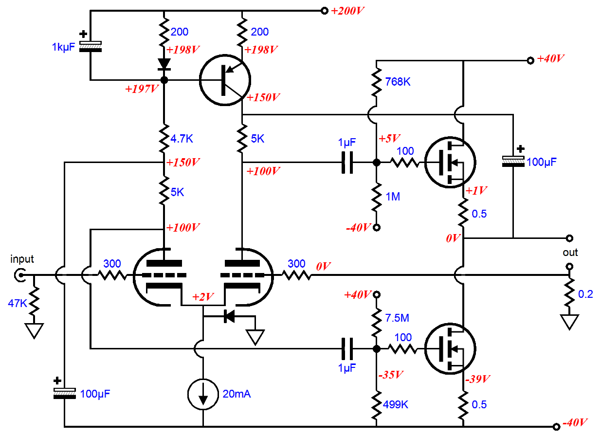
My fingers weary, so I will stop at this last variation, which is a hybrid affair based on this topology.
This is a power V-to-I amplifier that could drive loudspeakers, but, with wimpy MOSFETs and lower power supply voltages, a supremely fine headphone amplifier could be made, say +/-30Vdc and +150Vdc. Since one of the aims of a V-to-I amplifier is a near infinite output impedance, the inclusion of the DC current mirror at the top of the tube differential amplifier stage doesn't drag down the output impedance as a simple series 5k resistor would. (I don't actually believe that 5k is a big deal; I just wanted to strut my funky—design acumen—stuff.)
Next Time
* Capacitor Size
//JRB |
I know that some readers wish to avoid Patreon, so here is a PayPal button instead. Thanks.
John Broskie
E-mail from GlassWare Customers
High-quality, double-sided, extra thick, 2-oz traces, plated-through holes, dual sets of resistor pads and pads for two coupling capacitors. Stereo and mono, octal and 9-pin printed circuit boards available.  Aikido PCBs for as little as $24 http://glass-ware.stores.yahoo.net/
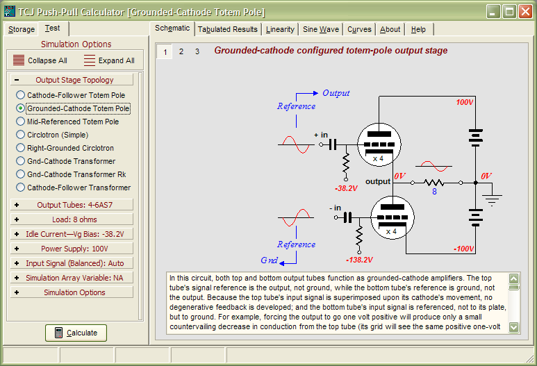
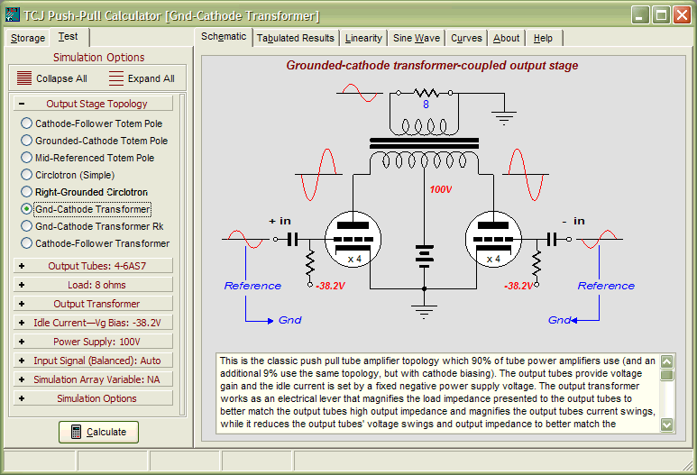
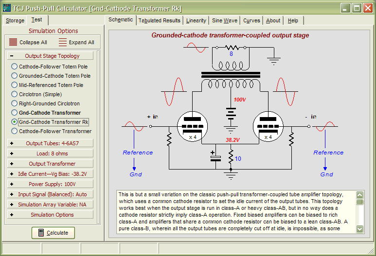
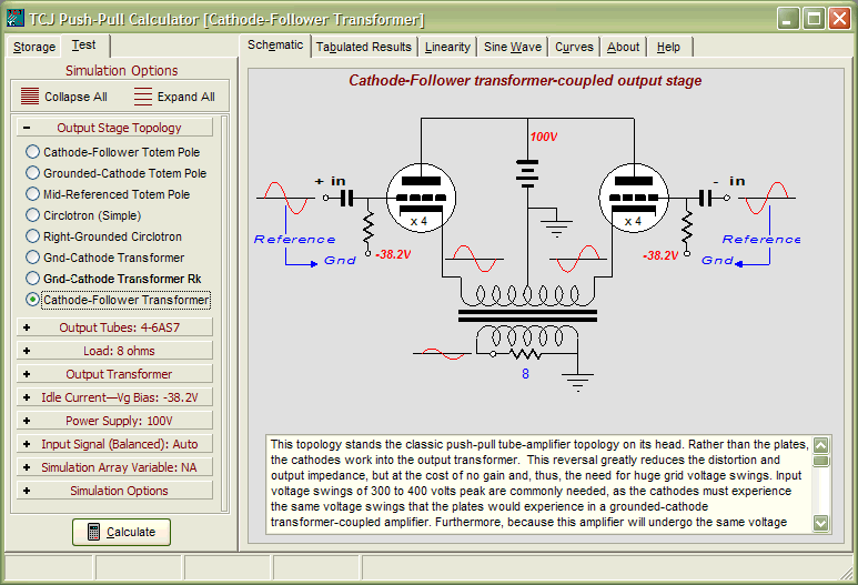
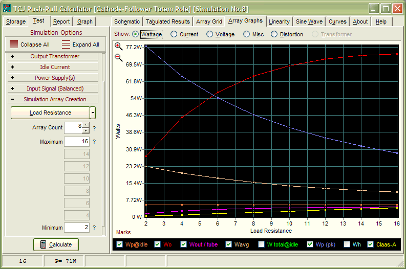
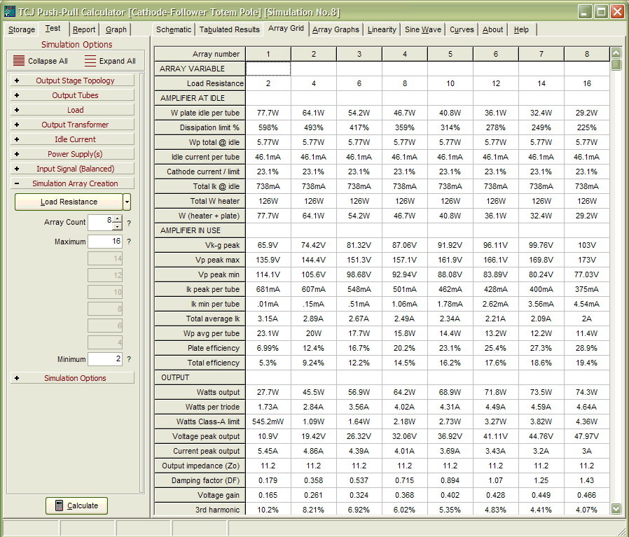
Support the Tube CAD Journal & get an extremely powerful push-pull tube-amplifier simulator for TCJ Push-Pull Calculator
TCJ PPC Version 2 Improvements Rebuilt simulation engine *User definable
Download or CD ROM For more information, please visit our Web site : To purchase, please visit our Yahoo Store: |
|||


| www.tubecad.com Copyright © 1999-2011 GlassWare All Rights Reserved |