| John Broskie's Guide to Tube Circuit Analysis & Design |
12 December 2016 Post 364
Single-Ended
It is by necessity pure class-A and it offers a constant output impedance due to its constant-transconductance operation. A push-pull output stage, in contrast, is most often run in class-AB, as it allows for greater power output and lower heat dissipation at idle, which in turn allows for smaller heatsinks and power transformers. The problem with class-AB lies in the output devices idling near their cutoff, where they are less linear. In addition, the region of device overlap, where both output devices are on at the same time results in gm doubling, which halves the output impedance in the overlap zone of operation (the class-A window of operation) and creates two transition points, where one device turns off during as the output voltage swings up and, then, the other device turns off on the downward swing. The problems we face with single-ended output stages are low output power, low efficiency, high heat dissipation, and, in the case of triode output tubes, poor PSRR. Seventeen years ago, in an article titled, Lowering the Single Ended Amplifier's Output Noise, I provided my solution to the last problem: poor PSRR. Since so few will follow links within a paragraph, here is a longish quote from that article.
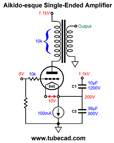
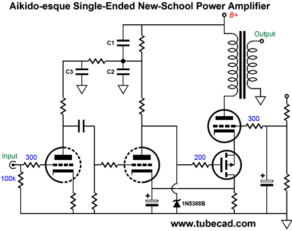
My solution was to purposely inject a portion of the power-supply noise into the output triode's cathode, which would then counter the power-supply noise at the B+ connection. In other words, we want the output triode to exhibit a constant-current draw in the face of power-supply noise, as the output transformer's primary is a current-variation-sensitive device. No current variation into the primary, no output signal on the secondary.
Capacitors, C1 & C2, define an AC voltage divider. By making C2 mu (triode's amplification factor) times larger than C1, we achieve the magic ratio that results in a power-supply-noise null. For example, a 6BX7, with a mu of 10, would require that C2's value be 10 times greater than C1's value. The constant-current source is not essential, as a simple cathode resistor could be used in its stead. It is, however, essential in the following design.
I came up with the above design in an e-mail exchange with a reader, Doan, from Viet Nam, who wants to run his single-ended output tube in class-A2, wherein the output tube experiences positive grid voltage.
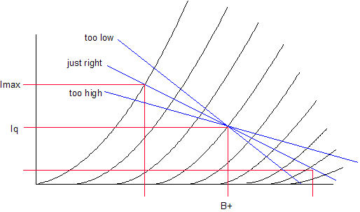
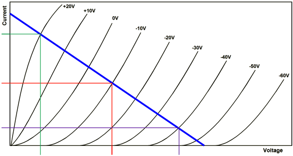
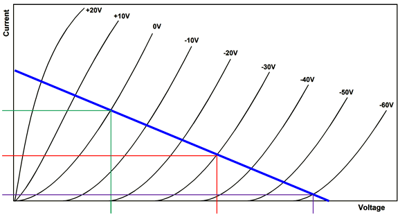
Class-A2 operation allows us to use a lower B+ voltage, run a higher idle current, and use a lower primary impedance than is usual in a single-ended amplifier, i.e. one that never runs into positive-grid voltages. For example, note how if we limited ourselves to no positive grid voltages in the above graph, the red idle-current plotline would have to be moved to the right and lower, while the load-line would have to be less steep.
Sounds great, so what is the problem? Grid current. The output tube must have a grid resistor, which is the resistor
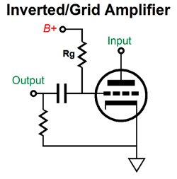
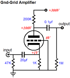
that spans from "ground" to the grid, and which provide the DC voltage path to either ground (or the negative bias voltage). We can readily measure this resistance; usually it's some value between 100k to 1M. The triode's grid, on the other hand, does not present a constant resistance, as its resistance depends on the voltage between the grid and the cathode and the voltage between the plate and cathode. In general, if the grid is at least one volt—or there about—more negative than the cathode, then the grid's resistance is nearly infinite, as the grid and cathode define a diode that is not forward biased. There is, in fact, a fundamental circuit topology that almost no one knows about: the inverted- or grid- amplifier. The way it works is that we use the grid as the "plate" and the plate as the "grid."
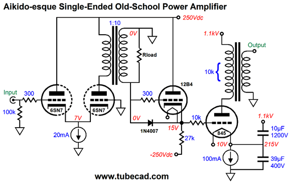
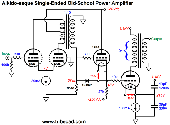
See http://www.tubecad.com/email_2001/e0829/page18.html for some details. But any way you slice it, there will be a sharp discontinuity between negative grid resistance and positive grid resistance. The big problem in most tube-audio amplifiers is that the coupling capacitor will become excessively charged up when the grid begins to conduct, which causes "blocking distortion." See Coupling-Capacitor Blocking Distortion in post 287. The 6SN7 input tube was configured as a cathode-coupled amplifier. Because the inter-stage transformer's primary presents so low a DC resistance, we do not have to worry about the problem of dissimilar plate voltage in the cathode-coupled amplifier. We do, however, have to worry about DC current flowing through the primary, which means that the inter-stage transformer must hold a air-gap. This might prove to be a pain, so the following variation makes use of a center-tapped primary, which means that the inter-stage transformer never experiences any net DC current flow and thus no net magnetizing of its core.
The resistor labeled Rload is needed not provide a path to ground, but to give the inter-stage transformer a load resistance to bite on. Since the winding ratio between primary and secondary is 1:10, the impedance ratio is 1:100 between winding (the voltage and current ratios are 1:10). Thus, a 100k load resistor will be reflected back to the primary as 1k, which would prove too low for the 6SN7. We could use a larger-valued load resistor, but then the inter-stage transformer would not be happy. Remember that inductive devices are in many ways the inversion of capacitors. Where a capacitor resists a change in the voltage across it, an inductor resists a change in current flow through it; where capacitors hate low-impedance loads, transformers and chokes love them, but hate high-impedance loads. So, lets make the inter-stage transformer happy by feeding its primary from a low-impedance source: a cathode follower.
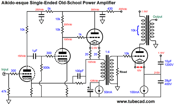
A 2A3 is used in the cathode-follower position, but many other tubes could be used, such as the 6BL7 or 6H30 or ECC99. The 2A3, on the other hand, would look cool. Whichever tube is used, it must get its own floating heater power supply, as the cathode must swing +/-200V voltage swings, which would exceed the triode's maximum cathode-to-heater voltage. Note that the inter-stage transformer winding ratio has dropped to 1:4, which means a new impedance ratio of 1:16. Also note that the loss in step-up of gain is made up by the input stage, which now holds two ECC99 triodes in cascading grounded-cathode amplifiers. Moreover, a negative feedback loop extends from the input tube to the cathode-follower's output, resulting in an even lower output impedance for the inter-stage transformer. Once again, a constant-current source is used to set the 2A3's idle current; once again, it proves essential, as it allows for variations in the second ECC99's plate voltage. The electrolytic capacitor that shunts the constant-current source must be large enough in value to prevent compromising the cathode-follower's output impedance. The 100pF feedback capacitor improves the input and driver stage phase margin. All in all, a very interesting circuit, one that I would love to hear in person. If I ever travel to Viet Nam, who knows, I just might have the chance.
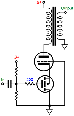
Grounded-Grid Single-Ended Output Stage We can, however, use a source follower (emitter follower) to drive the output tube's cathode.
The P-Channel MOSFET offers a much higher input resistance than the PNP transistor, but present much higher capacitance. The Fairchild FQP3P50 is a -500V/85W MOSFET that cost about $2 each. Ideally, the MOSFET should never come close to seeing its 500V source-to-drain voltage. Still, I wish that 1kV P-channel MOSFETs were made. The highest-voltage P-channel MOSFETs that I have seen are made by IXYS and are only rated for -600V. One problem we face with the above circuit is that the output triode cannot be driven positively. (For some, this might be a feature.) In order to get the cathode more negative than the grid (effectively making the grid positive relative to the cathode), we need to bias the grid up to some positive voltage, say +20V to +50V.
In the above schematic, we see the output tube's grid sitting at some positive voltage. We also see the driver triode's cathode terminating into the MOSFET's drain resistor. Why? This establishes a DC negative feedback loop, so that we can auto-bias the output tube. If the output tube conducts too much current, the driver triode conducts less, which forces the output tube's cathode more positive, which in turn lowers the output tube's current flow. Conversely, if the output stage conducts too little, the driver triode conducts more heavily, which pulls down its plate voltage, which pulls down the output tube's cathode voltage, which increases the output tube's current flow. The 1N5388B zener sets a limit how high the driver stage triode's plate can go positively, for those cases when the input and driver tube is missing from its socket. Another problem we face is that we cannot use my Aikido-esque PSRR enhancement technique—or can we? All we have to do is mix the correct portion of B+ noise into the signal we deliver to the MOSFET's gate. Yes, this is a seemingly paradoxical example of poor PSRR in the driver stage leading to better PSRR at the speaker. Capacitors C1 & C2 set the ratio of power-supply noise at the top of the plate resistor. Then the plate resistor and the second ECC99 triode define a two-resistance voltage divider. If you are getting that queasy feeling that a bunch of thick equations will follow, rest at ease.
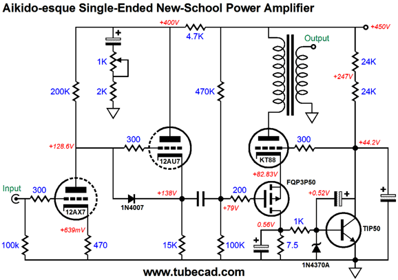
Doing voltage division with capacitors is difficult, as tight tolerance capacitors are both rare and expensive. This the reason I always prefer using two resistors over two capacitors. The above circuit makes use of a potentiometer to allow easy fine tuning of the PSRR null. Note the placement of the potentiometer below the capacitor. Electronically, it could just as well been placed atop the capacitor. In terms of potential-shocks, placing it below is much safer. True, such a mechanical failure is rare, but is not impossible. Another change is the replacement of the DC coupling between driver and output stage with a coupling capacitor. Now, I am less nervous about the P-channel MOSFET's life expectancy. We, nonetheless, retain auto-bias for the output stage, as the NPN TIP50 transistor's base monitors the voltage drop across the MOSFET's drain resistor, adjusting the output tube's grid voltage in its attempt to maintain a fixed voltage across this resistor. Yes, the TIP50 is rather long in the tooth, but I own a bunch of them. For less than one dollar, you can buy a Fairchild FJP5027 800V/50W NPN transistor.
Hybrid Single-Ended Designs
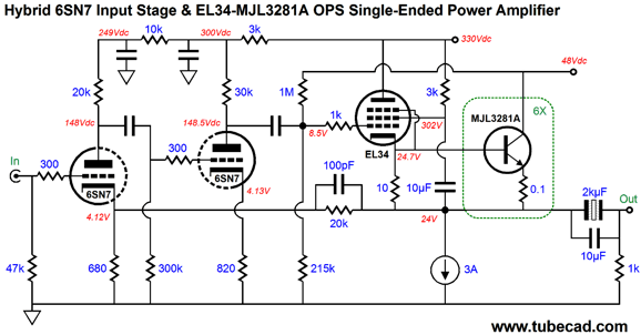
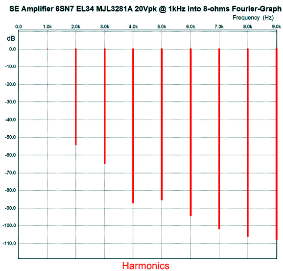
Two stages of gain followed by a hybrid buffer stage. The cascaded 6SN7 triodes provide all the signal gain. The EL34 is pentode connected and, along with six MJL3281 200W NPN transistors, drives the 8-ohm loudspeaker. A negative feedback loop ensures low distortion and low output impedance. The 3A constant-current source allows up to 24Vpk into 8-ohm loads. A more realistic goal, however, would be +/-20Vpk into 8-ohms. The output coupling capacitor, a non-polarized electrolytic capacitor, is bypassed by a 10µF film capacitor. Why so many output transistors? I wanted to keep each transistor's dissipation below 12W. In addition, it is much easier for a long heatsink to wick away heat from six evenly-spaced transistors than from just one super hot transistor at its center. In SPICE simulations, the above circuit worked well, very well. The output impedance is a low 0.11 ohms and the distortion at 20Vpk (25W) is far below 1%, as shown below.
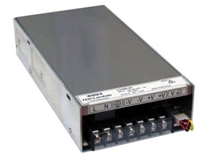
For those who don't like the EL34, a 300B or KT88 could be used instead. In fact, I would put my money on the bet that a kT77 would work best. Rather than use a wallwart or desktop 24V or 48V switcher power supply, we could use an enclosed version. TDK-Lambda's LS200-48 is a $58 48V @ 4.2A enclosed switcher.
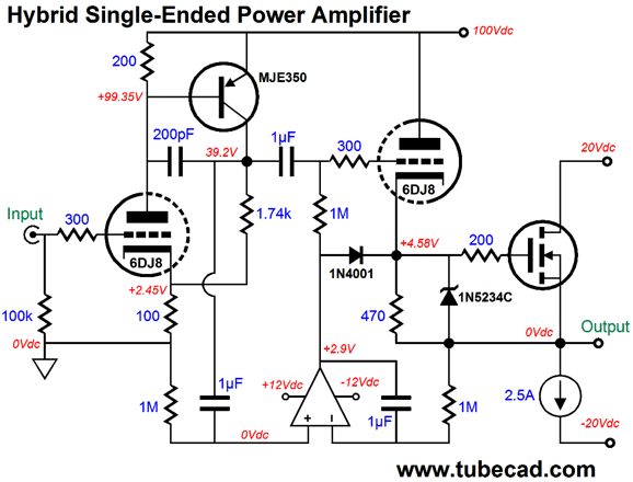
Certainly, a cheaper switcher could be bought, but a nice feature of the LS200-48 is its non-perforated enclosure. Why is this a feature? Ideally, we would like to keep its high-frequency noise inside its box. While looking through my single-ended schematics, I found the following design, which I created for a post last year, but never used (at least I think that I haven't posted it before).
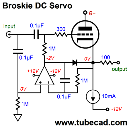
I could easily spend an entire post on explicating this circuit fully. Instead, let me quickly point out the highlights. The input 6DJ8 and MJE350 transistor define a two-stage compound amplifier that delivers a fixed gain of 16. The 200pF capacitor improves the phase margin of this compound amplifier. The second 6DJ8 triode is configured as a cathode follower that drive both the output and the N-channel MOSFET. The 1N5234C zener prevents the MOSFET from drawing excessive current. The 2.5 constant-current-source load allows swings of +/-16Vpk (16W) into 8-ohm loads. The Broskie DC servo loop keeps the output DC-offset free.
The Broskie DC servo protects the speaker should the 6DJ8 fail or be missing from its socket or just being cold. The diode only enrages when the cathode voltage falls below the OpAmp's output voltage. With a cathode follower, this would prove a problem, as the cathode must make +/-20Vpk swings. This is where the second 0.1µF capacitor at the input comes into play. It feeds the AC signal into the OpAmp's non-inverting input, so the OpAmp's output follows the input signal. At 16W output, the distortion looks almost identical to that produced by the previous hybrid circuit. If I were to actually build this amplifier, I would use at least two MOSFETs per channel, which would no doubt lower the distortion further.
Mixed-Mode Output Stage
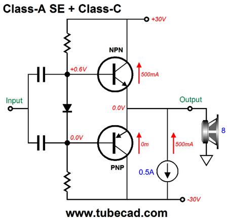
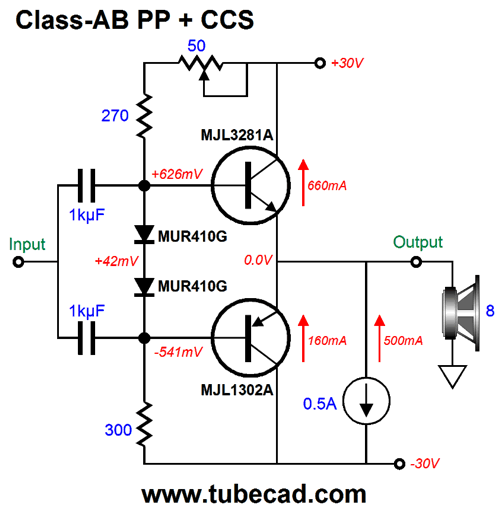
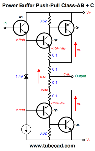
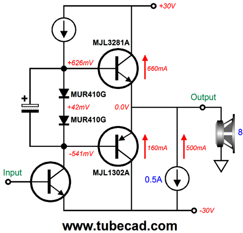
Doesn't look interesting? Perhaps not, but wait. I ran a SPICE simulation on the circuit and I noticed a small vertical line in the bottom half of the sine wave, where the NPN transistor had cut off, but the PNP had not yet begun to conduct, but where the constant-current source still pulled the output voltage down. The opposite of a crossover notch, more of a crossover slide. The workaround was obvious: just place another diode in series with the existing one, so the PNP transistor will turn on sooner.
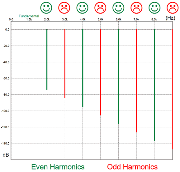
Well, I didn't get what I wanted, as the PNP transistor turned on at idle, drawing 160mA. What the heck, I thought and I ran a SPICE simulation. At first, I was disappointed by the resulting Fourier graph, as it showed a typical push-pull output stage harmonic structure. I was wrong. As I peered into the plotlines, I realized that this was not what I expected at all. Let start at the beginning. Single-ended (and the best class-A push-pull) output stages exhibit the following progression from 2nd to 9th harmonic of the fundamental frequency.
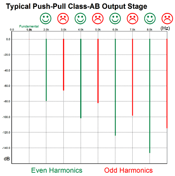
I have marked the nice-sounding even-order harmonics with happy faces and the icky-sounding odd harmonics with sad faces. The 3rd harmonic makes for a dead, dull sound; the 5th, a strident, edgy sound; the 7th and 9th, for a distressing metallic sound. (I highly recommend that you visit the Mathemagicalmusic website for more information on harmonics.) The typical push-pull output stage, whether tube or solid-state based, produces the following progression, where even harmonics fall further than odd harmonics.
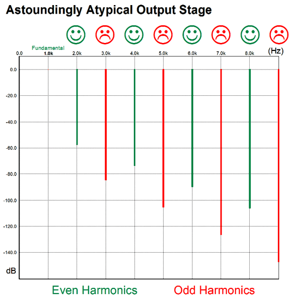
What I was seeing was similar, a jagged saw-tooth, but something radically different, much like a man biting a dog.
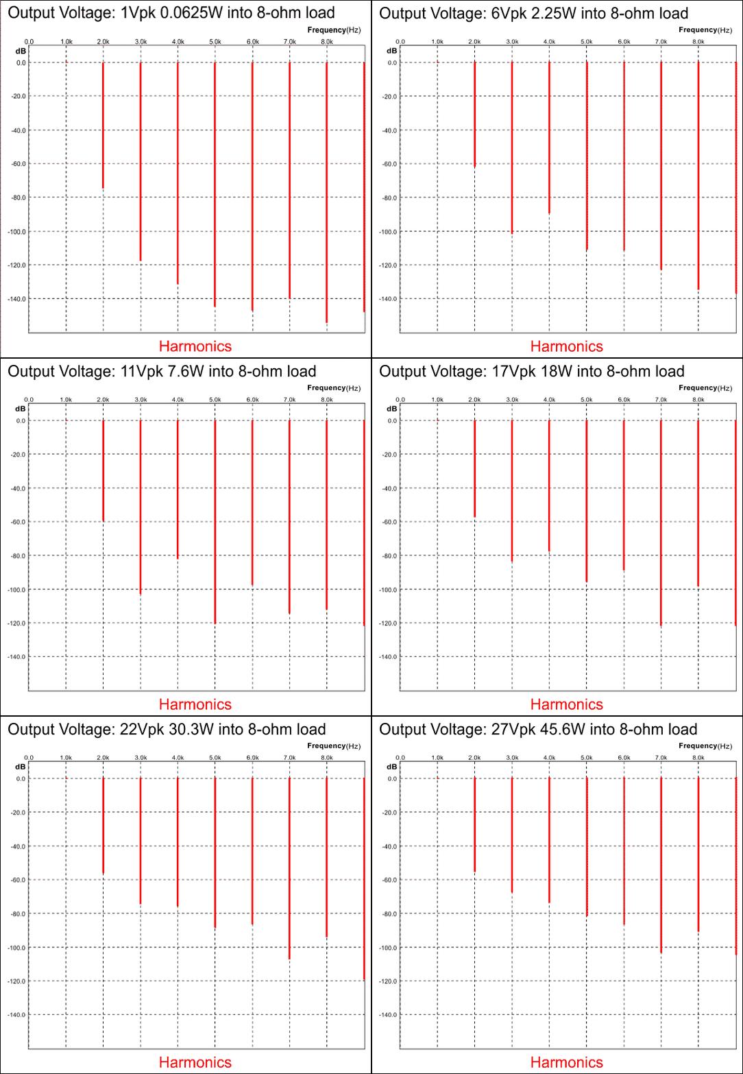
Without my color-coding, it was easy to think I was seeing the same old same thing. I wasn't. There was biting, but the man wasn't getting bit. Here is an animated GIF I created of the 28 SPICE simulations I ran with 1V input signal increments.
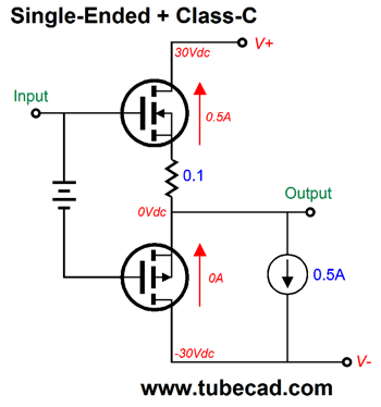
Altogether interesting, no? Understand that this isn't the same thing as the class-AB plus class-C from post 333.
Nor is it the single-ended plus class-C from the same post, as the PNP transistor is not cut off at idle, but draws a healthy 160mA.
Nor is it the quasi-single-ended quasi-class-G amplifier from post 362.
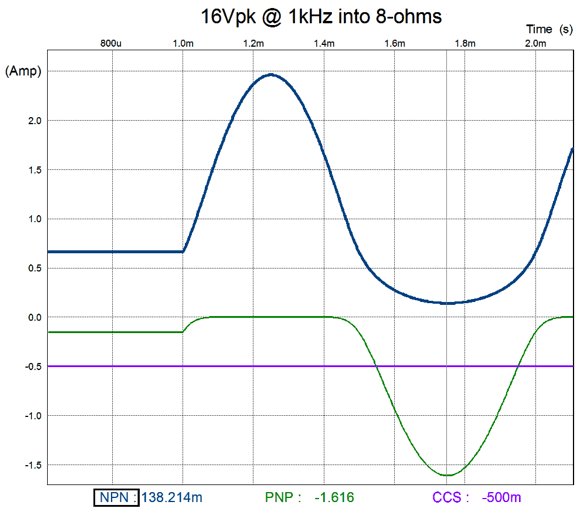
Instead, it is robust class-AB, push-pull operation plus a constant-current source. Indeed, this output stage does not neatly fit in any usual classification, as is revealed by the following graph.
Here the thick blue plotline belongs to the NPN transistor; the green line, the PNP transistor; and the violet line, the constant-current source. We are only looking at current flows here, no voltages. Note how the NPN device never turns off, the PNP transistor certainly does. Also note the asymmetry, as the NPN transistor must pass a peak of 3A, while the PNP transistor only has to pass a peak of a little more than 1.6A, while the 8-ohm load sees a peak current flow of 2A. Okay, now it is your turn, What class does this output stage operate in? Of course, if this output stage were nested within a power amplifier, no coupling capacitors would be needed.
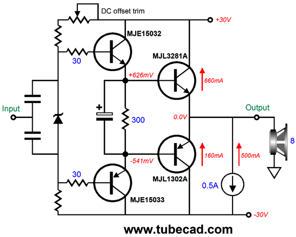
Note that the constant-current source that feeds the diode string must run hot, say 100mA. One workaround is to use a driver stage made up of an MJE15032-MJE15033 pair. In fact, using such a pair of driving transistors would allow us to use the coupling capacitors, but much smaller ones in value, so that we could drive the output stage with a typical tube-based line-stage amplifier.
Surprisingly enough, this version yielded even lower distortion than the previous version. Strangely enough, my added attempts to improve the circuit further by adding emitter resistors and cascoding the NPN output transistor only undid the inverted harmonic structure, wherein the odd harmonics fall further than the even harmonics.
Special Thanks
//JRB
User Guides for GlassWare Software Since I am still getting e-mail asking how to buy these GlassWare software programs:
For those of you who still have old computers running Windows XP (32-bit) or any other Windows 32-bit OS, I have setup the download availability of my old old standards: Tube CAD, SE Amp CAD, and Audio Gadgets. The downloads are at the GlassWare-Yahoo store and the price is only $9.95 for each program. http://glass-ware.stores.yahoo.net/adsoffromgla.html So many have asked that I had to do it. WARNING: THESE THREE PROGRAMS WILL NOT RUN UNDER VISTA 64-Bit or WINDOWS 7 & 8 or any other 64-bit OS. One day, I do plan on remaking all of these programs into 64-bit versions, but it will be a huge ordeal, as programming requires vast chunks of noise-free time, something very rare with children running about. Ideally, I would love to come out with versions that run on iPads and Android-OS tablets.
//JRB |
Kit User Guide PDFs
And
High-quality, double-sided, extra thick, 2-oz traces, plated-through holes, dual sets of resistor pads and pads for two coupling capacitors. Stereo and mono, octal and 9-pin printed circuit boards available.
Designed by John Broskie & Made in USA Aikido PCBs for as little as $24 http://glass-ware.stores.yahoo.net/
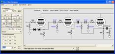
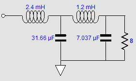
The Tube CAD Journal's first companion program, TCJ Filter Design lets you design a filter or crossover (passive, OpAmp or tube) without having to check out thick textbooks from the library and without having to breakout the scientific calculator. This program's goal is to provide a quick and easy display not only of the frequency response, but also of the resistor and capacitor values for a passive and active filters and crossovers. TCJ Filter Design is easy to use, but not lightweight, holding over 60 different filter topologies and up to four filter alignments: While the program's main concern is active filters, solid-state and tube, it also does passive filters. In fact, it can be used to calculate passive crossovers for use with speakers by entering 8 ohms as the terminating resistance. Click on the image below to see the full screen capture. Tube crossovers are a major part of this program; both buffered and un-buffered tube based filters along with mono-polar and bipolar power supply topologies are covered. Available on a CD-ROM and a downloadable version (4 Megabytes). |
||
| www.tubecad.com Copyright © 1999-2016 GlassWare All Rights Reserved |

